
Business
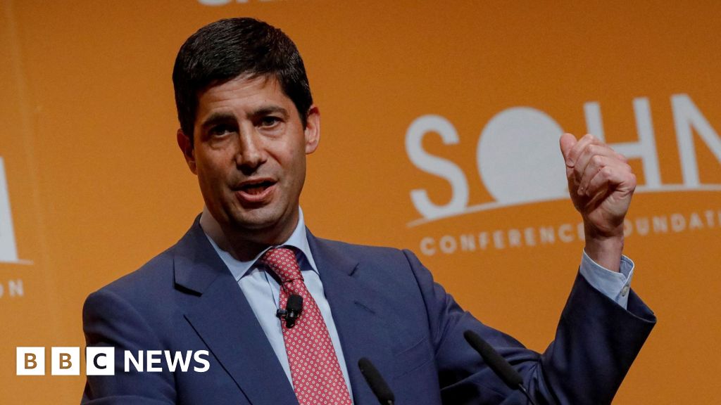
Who is Kevin Warsh, Trump's pick for Fed chair?


Daniel is an avid and active professional investor.
He runs Crude Value Insights, a value-oriented newsletter aimed at analyzing the cash flows and assessing the value of companies in the oil and gas space. His primary focus is on finding businesses that are trading at a significant discount to their intrinsic value by employing a combination of Benjamin Graham’s investment philosophy and a contrarian approach to the market and the securities therein. Learn more.
Analyst’s Disclosure: I/we have no stock, option or similar derivative position in any of the companies mentioned, and no plans to initiate any such positions within the next 72 hours. I wrote this article myself, and it expresses my own opinions. I am not receiving compensation for it (other than from Seeking Alpha). I have no business relationship with any company whose stock is mentioned in this article.
Seeking Alpha’s Disclosure: Past performance is no guarantee of future results. No recommendation or advice is being given as to whether any investment is suitable for a particular investor. Any views or opinions expressed above may not reflect those of Seeking Alpha as a whole. Seeking Alpha is not a licensed securities dealer, broker or US investment adviser or investment bank. Our analysts are third party authors that include both professional investors and individual investors who may not be licensed or certified by any institute or regulatory body.

Gold prices fall amid conflicting Iran war signals
Business
Gold below Rs 1.5 lakh, silver down Rs 2,000 on dollar strength, Trump’s power plant threat to Iran. What should investors do?

Tensions intensified on Sunday after US President Donald Trump issued a sharply worded Easter Sunday social media post directed at Tehran. He warned that Iran’s power plants and bridges could be targeted on Tuesday if the strategic Strait of Hormuz is not reopened.
MCX silver futures due May 2026 were down Rs 2,030 or 1% to Rs 2,30,465 per kg. Meanwhile, gold futures for June 2026 delivery fell Rs 1,047 or 0.7% to Rs 1,48,633 per 10 grams. In the previous session, the white metal plunged nearly 5% while gold ended marginally lower.
In the international market, gold prices declined sharply on Monday, falling more than 1%. Spot gold dropped 1.2% to $4,620.68 per ounce as of 0047 GMT, while U.S. gold futures for April delivery slipped 0.7% to $4,647.10. Meanwhile, spot silver also moved lower, declining 1% to $72.28 per ounce.
Market expectations around monetary policy have shifted significantly, with traders now largely pricing out the possibility of any rate cuts this year. Prior to the Iran war, there were expectations of two rate reductions during the year.

How should you trade gold?
Manoj Kumar Jain of Prithvi Finmart said precious metals are witnessing heightened volatility, although both gold and silver are expected to hold key support levels in the near term. He noted that silver could sustain above $62 per troy ounce, while gold may hold the $4,420 level on a closing basis this week.
He added that prices are likely to remain volatile amid fluctuations in the dollar index, crude oil prices, and the ongoing US-Iran conflict. For the current session, gold has support in the $4,620–4,580 range and resistance at $4,720–4,770 per troy ounce. Silver, meanwhile, has support at $70.70–68.00 and resistance at $76.00–78.40 per troy ounce.
On the domestic front, he said gold on MCX has support at Rs 1,47,200–1,45,500 and resistance at Rs 1,51,100–1,53,350. Silver is seen finding support at Rs 2,28,000–2,22,400, while resistance is placed at Rs 2,37,700–2,42,200.
Jain advised investors to consider booking profits in long positions on every rise and to wait for corrective dips before initiating fresh long positions in gold and silver.
Gold rates in physical markets
Gold Price today in Delhi
Standard gold (22 carat) prices in Delhi stand at Rs 1,10,792/8 grams while pure gold (24 carat) prices stand at Rs 1,20,856/8 grams.
Gold Price today in Mumbai
Standard gold (22 carat) prices in Mumbai stand at Rs 1,10,672/8 grams while pure gold (24 carat) prices stand at Rs 1,20,736/8 grams.
Gold Price today in Chennai
Standard gold (22 carat) prices in Chennai stand at Rs 1,11,592/8 grams while pure gold (24 carat) prices stand at Rs 1,21,736/8 grams.
Gold Price today in Hyderabad
Standard gold (22 carat) prices in Hyderabad stand at Rs 1,10,672/8 grams while pure gold (24 carat) prices stand at Rs 1,20,736/8 grams.
(Disclaimer: Recommendations, suggestions, views and opinions given by the experts are their own. These do not represent the views of The Economic Times)
Business
Cristiano Ronaldo’s Hamstring Injury Recovery Raises Questions on 2026 World Cup Performance Impact

LISBON, Portugal — Cristiano Ronaldo’s recent hamstring injury has sparked debate over whether the 41-year-old superstar can deliver peak performance at the 2026 FIFA World Cup, though Portugal coach Roberto Martinez and club updates suggest the setback poses minimal long-term threat to the five-time Ballon d’Or winner’s participation or output.

Ronaldo sustained the right hamstring injury on Feb. 28, 2026, during Al-Nassr’s Saudi Pro League match against Al-Fayha, forcing him to limp off the field. The club initially described it as a muscle issue requiring rehabilitation, with early estimates of two to four weeks sidelined. Al-Nassr coach Jorge Jesus later noted the injury appeared more serious than first thought after further tests, prompting Ronaldo to travel to Madrid for specialized treatment.
The timing raised eyebrows. With the World Cup set to kick off June 11 in the United States, Canada and Mexico, the injury came just months before what could be Ronaldo’s sixth and final appearance on football’s grandest stage. He missed Portugal’s March friendlies against Mexico and the United States as a precaution, heightening concerns among fans about his fitness at an age when recovery typically slows.
Yet recent developments paint a more optimistic picture. By early April 2026, Ronaldo had returned to full training with Al-Nassr. On April 3, he marked his comeback in style, scoring a brace — including a penalty and a powerful strike — in a 5-2 victory over Al-Najma. The performance pushed his official career goal tally to 967, edging closer to the landmark 1,000. Fabrizio Romano and other reporters confirmed Ronaldo is now available for club duty and expected to rejoin the Portugal squad without issue.
Martinez has repeatedly downplayed the concerns. “Cristiano’s injury is similar to those of Ruben Dias and Nelson Semedo. He is recovering well, and this is not an issue that should raise doubts about his participation in the World Cup,” the coach said after Portugal’s warm-up matches. He emphasized that the squad has about 60 days to monitor all players and described the problem as a minor muscle injury, not a threat to Ronaldo’s place. “The World Cup is not at risk. He is not at risk,” Martinez added.
Ronaldo himself shared positive updates on social media, posting gym photos with the caption “Getting better every day.” His legendary work ethic — often cited as the foundation of his longevity — remains evident. Even at 41, he maintains elite conditioning through rigorous routines, a factor Martinez highlighted when praising the forward’s physical shape this season.
The injury’s potential impact on performance is multifaceted. Hamstring strains can affect speed, acceleration and explosive movements critical for a striker like Ronaldo, who relies on bursts to beat defenders and finish chances. A grade 1 or mild grade 2 strain typically heals within weeks with proper rehab, but incomplete recovery risks re-injury or reduced sharpness. At Ronaldo’s age, experts note that muscle resilience diminishes, making prevention and gradual return essential.
Portugal’s Group K includes DR Congo, Uzbekistan and Colombia, with matches starting June 17 against DR Congo in Houston. Ronaldo scored five goals during qualifying, underscoring his enduring value. While younger talents like Bruno Fernandes, Bernardo Silva and Rafael Leao provide creative firepower, Ronaldo’s leadership, aerial ability and penalty prowess remain central to Portugal’s ambitions. Many analysts argue the team plays with greater confidence when their captain is on the pitch, even if his starting minutes are managed.
Historical context bolsters optimism. Ronaldo has overcome numerous injuries throughout his career, including hamstring issues at Real Madrid and Juventus. His ability to return stronger — often through sheer determination and science-backed recovery — is well-documented. In the Saudi Pro League this season, he has been Al-Nassr’s top scorer with 23 goals in 22 appearances before the layoff, demonstrating sustained form.
Still, some observers caution that cumulative wear could influence his World Cup output. Ronaldo has played over 1,200 senior matches, a staggering workload. Reduced explosiveness might limit his pressing or late-game impact, prompting Martinez to rotate more or deploy him as a focal point rather than a constant runner. Portugal’s depth allows flexibility; the side advanced comfortably without him in March friendlies.
Public reaction mixes concern with unwavering faith. Social media buzzed with #Ronaldo2026 hashtags during his absence, while his comeback brace quieted many doubters. Supporters point to his record: top scorer in qualifying, consistent club contributions and unmatched mental fortitude. Critics, however, highlight the realities of age, noting that even icons like Lionel Messi have seen physical decline in later years.
Medical perspectives vary. Typical hamstring recovery timelines suggest Ronaldo should be fully fit by mid-April, giving him nearly two months of competitive play before the tournament. Strength and conditioning programs focusing on eccentric loading and flexibility will be key to rebuilding confidence in the muscle. Portugal’s medical staff will collaborate closely with Al-Nassr to ensure a seamless transition.
Beyond individual performance, the injury narrative underscores broader themes in modern football: player longevity, load management and the balance between club and country duties. Ronaldo’s move to Al-Nassr in 2023 drew scrutiny over competitive level, yet he has thrived, using the league as a platform to chase records while preparing for international duty.
As April 2026 progresses, all eyes remain on Ronaldo’s minutes and output for Al-Nassr. A strong run of form would silence remaining doubts heading into Portugal’s final pre-tournament preparations. Martinez has made clear that selection hinges on current standards, not past glory — a benchmark Ronaldo has met throughout his career.
For Portugal, reaching the knockout stages and beyond depends on collective strength, but few doubt Ronaldo’s motivational role. Whether he starts every match or impacts as a substitute, his presence could prove decisive in tight contests against Colombia or in potential later rounds.
The 2026 World Cup offers Ronaldo a chance to add to his legacy as one of football’s greatest. While the hamstring episode briefly clouded the outlook, his swift return and positive signals suggest the setback will not significantly derail his performance. With months of monitoring ahead and his trademark dedication intact, the Portuguese icon appears on track to lead his nation once more on the global stage.
Football enthusiasts continue to debate the fine line between caution and optimism. Ronaldo’s body of work suggests he will arrive in North America ready to compete. As the tournament draws nearer, his fitness will be tracked daily, but early indications point to business as usual for one of the game’s most resilient figures.
Key Timeline:
- Feb. 28, 2026: Injury sustained vs. Al-Fayha
- March 2026: Missed Portugal friendlies
- Early April 2026: Returned to Al-Nassr training and scored brace
- June 11, 2026: World Cup begins
Portugal opens Group K play June 17 against DR Congo. For the latest on Ronaldo’s status and World Cup preparations, follow official FIFA and Portugal national team channels.

Prime Minister Anutin Charnvirakul initiated legal action against fuel smugglers to Cambodia, citing national security. The government plans to review fuel pricing amid rising costs and secure adequate reserves.
Key Points
- Prime Minister Anutin Charnvirakul has ordered strict legal action against illegal fuel smuggling to Cambodia, emphasizing its threat to national security and forming a task force for investigations and arrests.
- The government is exploring measures to mitigate rising fuel prices, with Deputy Prime Minister Ekniti Nitithanprapas advocating for a review of refining and marketing margins, aiming to submit proposals to the Cabinet on April 6.
- Thailand’s fuel reserves can meet demand for about three months, while global oil prices remain volatile. Bangchak Corporation has produced 35,000 liters of B20 diesel for distribution at service stations within April.
Prime Minister Anutin Charnvirakul has ordered strict legal action against those involved in smuggling fuel to Cambodia following the discovery of an illegal cross-border network. The premier directed the formation of a task force to investigate and arrest those responsible, warning that such activities would be treated as a threat to national security.
The order comes as the government considers measures to ease the impact of rising fuel prices. Deputy Prime Minister and Finance Minister Ekniti Nitithanprapas has called for a review of refining and marketing margins to help lower retail prices, with proposals set to be submitted to the Cabinet on April 6. The review includes reassessing cost calculations and setting appropriate margins.
Officials are also examining pricing components, including a war-related premium linked to tensions in the Middle East. Authorities said some costs currently included in fuel pricing may not fully align with actual supply conditions, as refineries source crude oil from multiple regions.
The Ministry of Energy reported that Thailand’s fuel reserves are sufficient for about 3 months of demand, with additional supplies being secured. Global oil prices remain volatile, while domestic diesel production continues to fall slightly short of consumption. The Oil Fuel Fund remains in deficit as subsidies are used to manage price pressures.
Separately, Bangchak Corporation has produced an initial batch of 35,000 liters of B20 diesel, which will be distributed through depots and made available at service stations within April for use in large diesel engines.
Source : Thai PM Orders Crackdown on Fuel Smuggling to Cambodia
Other People are Reading

This is the forum for daily political discussion on Seeking Alpha. A new version is published every market day.
Please don’t leave political comments on other articles or posts on the site.
The comments below are not regulated with the same rigor as the rest of the site, and this is an ‘enter at your own risk’ area as discussion can get very heated. If you can’t stand the heat… you know what they say…
More on Today’s Markets:
Moderation Guidelines:
We remove comments under the following categories:
- Personal attacks on another user account
- Anti-Vaxxer or covid related misinformation
- Stereotyping, prejudiced or racist language about individuals or the topic under discussion.
- Inciting violence messages, encouraging hate groups and political violence.
Regardless of which side of the political divide you find yourself, please be courteous and don’t direct abuse at other users.
For any issue with regards to comments please email us at : moderation@seekingalpha.com.
Seeking Alpha’s Disclosure: Past performance is no guarantee of future results. No recommendation or advice is being given as to whether any investment is suitable for a particular investor. Any views or opinions expressed above may not reflect those of Seeking Alpha as a whole. Seeking Alpha is not a licensed securities dealer, broker or US investment adviser or investment bank. Our analysts are third party authors that include both professional investors and individual investors who may not be licensed or certified by any institute or regulatory body.


Supermarkets, shopping centres, and more have reopened today, Easter Monday, but operating hours will vary depending on location.
It is therefore being encouraged to check a store operating hours for today before heading out.
What’s Open on Easter Monday
According to a report by Sky News, all Woolworths, Coles, and Aldi locations across Australia have reopened for Easter Monday. However, as previously mentioned, operating hours will vary.
As for Westfield, the following schedule will be implemented today:
- ACT – 10 a.m. to 4 p.m.
- NSW – varying hours
- SA – closed
- Victoria – 10 a.m. to 5 p.m.
- WA – 11 a.m. to 5.pm.
How About General Retail, Bottle Shops?
SBS News notes that the likes of Target, Kmart, Big W, and Bunnings will likewise open today. However, only selected stores in South Australia will be open.
Bottle shops, such as Dan Murphy’s, have also reopened today but with reduced hours.
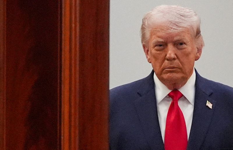

Trump vows ’hell’ for Iran if Strait stays shut, says a deal is possible
Business
ETMarkets Smart Talk | Nifty in ‘bounce zone’ as valuations fall below 10-year average; de-escalation key: Harendra Kumar

In an interaction with Kshitij Anand of ETMarkets, Harendra Kumar, Managing Director at Elara Capital, noted that the Nifty has entered a “bounce zone,” trading below its 10-year average valuation—a level that has historically acted as a strong support for markets.
He believes that while external shocks have weighed on sentiment, India’s underlying macro fundamentals remain resilient, and a swift de-escalation in geopolitical tensions could trigger a sharp rebound, setting the stage for a recovery in FY27. Edited Excerpts –
Q) Thanks for taking the time out. FY26 returns have turned negative due to geopolitical concerns around West Asia. How do you sum up the financial year?
A) FY26 was a year in which resilient domestic macro-economic fundamentals were overshadowed by external shocks. US reciprocal tariffs, AI disruption for Indian IT stocks and now the West Asian crisis has hemorrhaged the markets.
Given that the shocks are exogenous – flows have been severely impacted. Outflows at USD 19.7bn has been debilitating. However, there is a silver lining.
With all the noise of the INR depreciation and resultant worries – it has become reasonably valued. The trend of outflows should reverse at some point during the fiscal given this backdrop.
Q) As we head towards FY27, what are the key triggers investors should keep in mind that could lead to a market reversal or return of bullish sentiment?
A) Over the last two years valuations had been our Achilles heel. After the sharp cuts – the Nifty is in a bounce zone. At ~17.3x, Nifty trades 7% below its 10-year average of ~18.6x, placing it in a historical “bounce zone”.
Outside of extreme disruptions like COVID-19, this level usually acted as a floor for valuation. Even during the Russia–Ukraine conflict, despite Brent sustaining above USD 100/bbl, Nifty multiples bounced back from 10-year rolling averages.This is a big positive. With strong fundamentals – a quick de-escalation should see a whipsaw in the markets.
Q) Which sectors should be on investors’ radar for FY27?
A) Large-cap auto stocks, have corrected sharply, witnessing a ~17% drawdown since the onset of the US-Iran conflict. While near-term concerns persist around input cost pressures from elevated commodity prices and potential demand moderation in the event of a prolonged conflict triggering an inflation shock for consumers, underlying retail data remains robust and encouraging.
Additionally, 18 out of the 19 utility stocks under our coverage have outperformed the Nifty 50 in current drawdown, underscoring the sector’s relative resilience.
The escalating conflict is expected to accelerate India’s electrification cycle, while surging data centre capex is driving incremental power demand.
This positive backdrop is further supported by the likely passage of the New Electricity Amendment Bill, which will unlock structural reforms in the sector.
Consequently, power generation, transmission, distribution, and data centre-linked plays are emerging not merely as defensive anchors but as clear structural beneficiaries in the medium to long term.
Q) How should one approach gold and silver in the new financial year?
A) Gold is store of value and should stay that way. At some levels its also viewed as hedge. There could be a bounce trade once the dollar starts to weaken again but beyond that I am not sure whether we are going to see a rally like last year.
For country that is witnessing strong nominal growth and emergence of new sectors – stronger compounding exists in equities.
Q) Do you think there are certain sectors that have already corrected and are now available at attractive valuations?
A) Beyond Auto and Power – IT services, Banks and real estate offer meaningful valuation comfort.
Banks trade at ~1.4x P/B (FY28E), a ~31% discount to their 10-year median. Autos, post the recent correction, are at ~19.5x, about a 5% discount to the 5-year median, offering an attractive entry point.
IT services also stand out, at ~16.4x FY28 P/E, the sector trades at a 20%/31% discount to its 10-year/5-year medians, respectively. With no material disruption to revenue streams and margins so far from the AI transition, the medium-term risk-reward appears attractive.
Q) How are we positioned against peers in terms of valuations?
A) India still trades at a premium to peers, but the gap has normalised meaningfully from 2024 extremes. The MSCI India premium to MSCI EM has moderated to ~60%, closer to its 10-year average, from peaks above 100% in August 2024, indicating that excess froth has largely been corrected.
Even so, on a 2-year forward P/E basis, India at 15.7x remains above MSCI EM at 10.3x. This premium is partly justified by stronger fundamentals.
India offers ~22% USD EPS CAGR over CY25–27E with ~15.7% ROE, at par with most global markets. In contrast, China trades cheaper but with lower returns (~10.4% ROE), while Korea’s low valuations reflect a more cyclical and concentrated earnings profile.
Overall, India remains a premium market, but the premium now appears more aligned with its growth visibility, return profile, and macro stability.
Q) Will FII flows reverse in FY27? How are you interpreting both domestic and global flows?
A) Our base case is that FII flows can improve in FY27, but a sharp, linear reversal looks less likely.
Domestic fundamentals are turning supportive: nominal GDP is recovering, earnings growth is broadening, valuation premiums have moderated, and trade-related overhangs have eased.
Historically, FPI flows have tracked nominal growth cycles, which supports a gradual return. A durable reversal in FPI inflows will require three conditions: softer energy prices, a stable rupee, and continued earnings strength. Until then, flows are likely to improve in phases and remain episodic in nature.
(Disclaimer: Recommendations, suggestions, views, and opinions given by experts are their own. These do not represent the views of the Economic Times)

NEW YORK — The New York Times Wordle puzzle #1752 on Monday, April 6, 2026, challenged players with a five-letter word tied to solemn promises and legal oaths, testing vocabulary and strategic guessing in the enduring daily word game.

Wordle, the simple yet addictive online puzzle where players have six attempts to identify a hidden five-letter word, remains a morning ritual for millions worldwide. Created by Josh Wardle and acquired by The New York Times in 2022, the game delivers one new challenge each day with color-coded feedback: green for correct letters in the right position, yellow for correct letters in the wrong spot and gray for letters not in the word at all.
For Monday’s edition, the solution was SWORN. The word, the past participle of “swear,” commonly appears in contexts like “sworn testimony” or “sworn enemies,” referring to something affirmed under oath or pledged with conviction. According to dictionary definitions, it describes a commitment or declaration made solemnly, such as when a witness is “sworn in” before testifying in court.
Solvers who opened with strong starter words like “SLATE,” “CRANE” or “RAISE” often spotted the “S” and “N” early, narrowing possibilities quickly. One effective hint shared across gaming sites: the word begins with “S,” ends with “N,” contains just one vowel and features five unique letters with no repeats. It functions as both a verb form and adjective, with synonyms including “promised” and, in some usages, “cursed.”
Difficulty hovered around average for the puzzle, with many players reporting solves in three to four guesses. The New York Times’ internal data and community feedback placed the average around 3.9 attempts, making it neither the easiest nor toughest of recent weeks but still demanding careful elimination of wrong letters. Players who tried “SWORD” as a guess frequently saw useful yellow feedback on the “S,” “W” and “R,” guiding them toward the correct “SWORN.”
Wordle’s enduring appeal lies in its accessibility and lack of pressure — no timers, no ads interrupting play and a single puzzle shared globally each day. The sharing feature, which generates emoji grids of colored squares without spoiling the word, fuels social media conversations as friends and family compare streaks and strategies. On April 6, posts flooded platforms with everything from “three in a row” celebrations to lighthearted complaints about missing the oath-themed answer.
The puzzle arrived as Wordle continues evolving under NYT stewardship, with the company maintaining strict rules on acceptable solutions to keep gameplay fair and family-friendly. Monday’s word avoided obscure terms, sticking to common English while still offering a satisfying “aha” moment for those who connected it to courtroom dramas or solemn vows.
For those seeking hints before the full reveal, early clues included thinking about legal or formal commitments, focusing on words with a strong consonant structure and considering past-tense forms of common verbs. The word has more consonants than vowels, a trait that helped narrow guesses once initial attempts revealed the vowel placement.
Wordle #1752 followed Sunday’s puzzle, which featured “ENVOY,” continuing a streak of relatively straightforward but thoughtfully chosen words. Players maintaining long streaks appreciated the Monday offering, as “SWORN” rewarded logical deduction without relying on rare vocabulary. Educators often highlight such puzzles for building language awareness, pattern recognition and resilience when early guesses go awry.
The game’s popularity shows no signs of waning nearly four years after its viral explosion. Millions log in daily via the NYT Games app or website, where Wordle sits alongside Connections, Spelling Bee and Strands as part of a robust puzzle portfolio. Subscriptions unlock additional features, including unlimited practice puzzles and ad-free access, but the core daily Wordle remains free for all.
Community sites and gaming outlets like Rock Paper Shotgun, TheGamer and Forbes provided spoiler-free hints throughout the day, emphasizing starting words rich in vowels and common consonants. One tip that gained traction: “WORST” as an opener turned four letters yellow for many, dramatically cutting down possibilities and steering solvers toward success.
“Sworn” carries cultural weight beyond the grid. It evokes images of sworn officers, sworn statements in legal documents and even literary phrases like “sworn brothers” in tales of loyalty. Its Old English roots trace back to words meaning to take an oath, underscoring how everyday language preserves ancient traditions of truth-telling and binding promises.
As the workweek began, the puzzle offered a brief mental reset amid global news and busy schedules. For some, solving it in two or three tries boosted confidence heading into the day; for others, using all six attempts served as a reminder that persistence pays off. Wordle Bot analyses, popular among competitive players, often recommended “SLATE” or similar openers, which performed well against Monday’s consonant-heavy solution.
Looking ahead, the NYT Games team keeps the word list fresh and balanced, mixing common terms with occasional curveballs to maintain engagement. April 6’s edition exemplified the sweet spot: challenging enough to feel rewarding, familiar enough to avoid frustration.
Those who missed the solution or want to revisit can check the official NYT Wordle archive, though daily puzzles reset at midnight. New players benefit from the built-in tutorial that explains mechanics without overwhelming. The game encourages experimentation — trying unusual starters or focusing on letter frequency statistics — while reminding everyone that fun trumps perfection.
In an era of endless digital entertainment, Wordle’s stripped-down design stands out. No flashy graphics, no in-app purchases pressuring progress, just pure linguistic deduction shared across time zones. From bustling cities like New York to quiet mornings in South Korea, players aligned on the same five letters, fostering a quiet global camaraderie.
Monday’s “SWORN” delivered classic Wordle satisfaction with its blend of everyday usage and subtle depth. Whether nailed on the first try or solved on the final guess, it reinforced why the puzzle captivates: each green tile brings a small victory, each puzzle a fresh opportunity to sharpen the mind.
For the latest Wordle coverage, hints without spoilers and analysis of upcoming puzzles, enthusiasts turn to dedicated sections on The New York Times site or independent gaming resources. As streaks build and records fall, the game continues proving that sometimes the simplest ideas — guess a word, learn from colors, try again — create the most lasting habits.

Michael Saylor Hints at Return to Weekly Bitcoin Purchases

Sanjiv Goenka’s Unmissable Reaction Viral As Mohammed Shami And LSG Tear SRH Apart

iCloud email goes down for some users in an Easter Sunday outage


-

 NewsBeat3 days ago
Steven Gerrard disagrees with Gary Neville over ‘shock’ Chelsea and Arsenal claim | Football
-

 Business3 days ago
No Jackpot Winner and $194 Million Prize Rolls Over
-

 Fashion2 days ago
Weekend Open Thread: Spanx – Corporette.com
-
Entertainment7 days ago
Fans slam 'heartbreaking' Barbie Dream Fest convention debacle with 'cardboard cutout' experience
-
 Crypto World4 days ago
Gold Price Prediction: Worst Month in 17 Years fo Save Haven Rock
-

 Business5 hours ago
Three Gulf funds agree to back Paramount’s $81 billion takeover of Warner, WSJ reports
-
Crypto World6 days ago
Dems press CFTC, ethics board on prediction-market insider trades
-
 Sports1 day ago
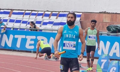
India men’s 4x400m and mixed 4x100m relay teams register big progress | Other Sports News
-

 Business4 days ago
Login and Checkout Issues Spark Merchant Frustration
-

 Tech6 days ago
EE TV is using AI to help you find something to watch
-

 Tech7 days ago
Apple will hide your email address from apps and websites, but not cops
-

 Sports6 days ago
Tallest college basketball player ever, standing at 7-foot-9, entering transfer portal
-
 Politics6 days ago
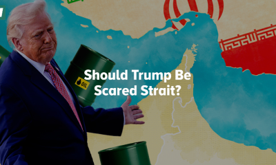
Should Trump Be Scared Strait?
-

 Tech6 days ago
Flipsnack and the shift toward motion-first business content with living visuals
-

 Fashion7 days ago
The Best Spring Trends of 2026
-
Tech6 days ago
Daily Deal: StackSkills Premium Annual Pass
-

 Crypto World6 days ago
U.S. rule change may open trillions in 401(k) funds to crypto
-

 Sports6 days ago
Women’s hockey camp eyes fitness boost, tactics ahead of WC 2026 campaign | Other Sports News
-

 Tech6 days ago
How to back up your iPhone & iPad to your Mac before something goes wrong
-
 Politics7 days ago
BBC slammed for ignoring author of The Fraud
You must be logged in to post a comment Login