Connect with us
DAPA Banner
DAPA Coin
DAPA
COIN PAYMENT ASSET
PRIVACY · BLOCKDAG · HOMOMORPHIC ENCRYPTION · RUST
ElGamal Encrypted MINE DAPA
🚫 GENESIS SOLD OUT
DAPAPAY COMING

Tech

Your next free Google account might only come with 5GB of storage

Published

on

Google has quietly altered one of the most reliable promises in consumer tech: 15GB of free cloud storage. For years, signing up for a Google account meant getting 15GB of free storage, shared across Gmail, Drive, and Photos. However, that’s changed. 

New accounts are now defaulting to 5GB (same as iCloud), with the full 15GB available only if you have entered your phone number during setup. The prompt users are seeing reads: “Your account includes 5GB of storage. Now get even more storage space with your phone number.”

What exactly changed?

The policy change took effect sometime around March 18, 2026 (via 9To5Google). That’s when the company updated its support page language from definitive to conditional. Initially, the support page read “Your Google account comes with 15GB of cloud storage at no charge.”

Now, it has been updated to say “up to 15GB of cloud storage at no charge.” And Google didn’t announce the change via a tweet or a blog post, as it does for every other update that comes out for consumer-centric products. 

It is during the account setup that users are now seeing two explicit choices: link a phone number to get 15GB of storage or keep 5GB. 

Advertisement

Why is Google doing this?

Google wants to make sure that the 15GB storage is offered to users only once, and not as many times as they create a new account. Linking the free storage to users’ phone numbers is, I’d say, a smart move, as it’s much more difficult to get a new number than to create a new Google account.

So, the company is positioning the change as an anti-duplication measure rather than anything else. A Google spokesperson has also confirmed to Endgadget that this is a regional test, which is why some users are still able to access the 15GB free storage without verifying their phone number. 

At the same time, I’d also like to draw your attention to the timing of this change. Only recently did Google expand the available storage for AI Pro subscribers from 1TB to 5TB, and now, it’s enforcing a tighter space for free users. Ultimately, we should all prepare for slimmer free storage margins.

Source link

Advertisement
Continue Reading
Click to comment

You must be logged in to post a comment Login

Leave a Reply

Tech

Jeff Bezos’ Blue Origin space venture reportedly considers seeking outside investment for the first time

Published

on

Blue Origin New Glenn rocket lifts off from Florida launch pad
Blue Origin’s New Glenn rocket lifts off from its Florida launch pad in April. (Blue Origin Photo)

For more than a quarter-century, Jeff Bezos has been funding his Blue Origin space venture primarily with his gains from Amazon, the other big company he founded — but according to a report in the Financial Times, Blue Origin is now weighing a plan to seek outside investment for the first time.

The report says Blue Origin CEO Dave Limp told employees at a recent all-hands meeting that the company might have to turn to external fundraising if it went ahead with plans to increase its launch cadence significantly. The Financial Times attributed its report to two unidentified sources who attended the meeting. We’ve reached out to Blue Origin for comment and will update this report with anything we hear back. The company doesn’t typically comment on claims attributed to unidentified sources.

Blue Origin launched its heavy-lift New Glenn rocket for the first time in January 2025, and two more New Glenn missions have followed since then. The most recent launch took place last month but failed to put its payloads in their proper orbit. As a result, New Glenn is grounded until the company completes an investigation and takes corrective actions under the oversight of the Federal Aviation Administration.

Past reports have suggested that Blue Origin was targeting as many as 12 New Glenn launches this year, and as many as 100 launches per year in the longer term.

Bezos founded his space venture in 2000. In 2017, he told reporters that his business model was to “sell about $1 billion a year of Amazon stock” and invest it in Blue Origin. Since then, the company has brought in revenue from suborbital spacefliers and researchers, commercial satellite operators and government agencies including NASA. One of the notable contracts was a $3.4 billion award to build a crew-capable lunar landing system for NASA.

Advertisement

But Blue Origin has billions of dollars in capital expenses to cover, including expanded manufacturing and launch facilities in Florida. It also has to compete for talent with SpaceX, which is planning an initial public offering that values the company at more than $2 trillion.

During the all-hands meeting, Limp reportedly referred to the potential for outside fundraising as he responded to questions about a new stock option plan for employees. The Financial Times quoted its sources as saying that Limp did not rule out a future IPO.

Source link

Advertisement
Continue Reading

Tech

Exciting courses to kick-start your career in future health

Published

on

Whether you are a professional, a student or a novice, there are plenty of opportunities open to those looking to expand their skills.

The medtech and future health ecosystem is excitingly broad in that there are a plethora of career routes open to students and professionals looking to advance. Whether your interests lie in AI, medical devices or regulation, SiliconRepublic.com has compiled a list of some of the most interesting courses designed to take professionals to that next phase of their careers. 

So, if you are looking to excel in a dynamic and ever-evolving space then read on to see if one of these educational opportunities is right up your alley. 

Coursera

For the professionals at the intersection between the healthcare and technology spaces, with plans to innovate for the future, Coursera has courses such as ‘AI in Healthcare’ specialisation.

Advertisement

This five-course series takes roughly four weeks to complete at 10 hours a week, is designed for beginners and can be engaged with a flexible schedule. Students will identify the problems that healthcare providers face, learn where machine learning can have an impact, analyse how AI affects patient care safety, quality and research, relate AI to the science, practice and the business of medicine, and “apply the building blocks of AI to help innovate and understand emerging technologies”.

Other courses on offer – some paid and some free – include ‘AI in Healthcare & Drug Discovery’, ‘Future Health: Digital Health and Healthcare Innovation’, and ‘Pharmaceutical and Medical Device Innovations’. Most of these courses come with an assessment at the end and a shareable certificate acknowledging the achievement. 

EIT Health

EU-backed healthcare, innovation and entrepreneurship network EIT Health currently has a paid course that would likely appeal to European professionals looking to further their understanding of regulation in the health-tech space.

The ‘Healthcare Regulations: Ensuring Regulatory Compliance by Design’ course is a little more costly than others on this list at €300, but the programme is self-paced, takes roughly a month to complete and can be engaged with entirely online.

Advertisement

This programme helps students understand how to integrate regulatory thinking into every step of product development, ensuring “technology is market-ready from day one”. Through real-world examples and case studies, students will learn how to design, test and validate medical devices that meet European standards while fostering a culture of innovation and safety.

It is designed for professionals and postgraduate learners in medtech, biotechnology and digital health who want to strengthen their ability to lead compliant innovation.

FutureLearn

On the FutureLearn website, the University of Leeds is offering several medtech-focused courses for those with more of a budget who are looking to expand their education.

One such course is the ‘MedTech: Orthopaedic Implants and Regenerative Medicine’ module. The introductory level programme is two-weeks long, requires about 10 hours total and comes with a certification of accreditation at the end. In this course, students will learn about how medtech is used in orthopaedics and how the benefits of regenerative medicine will affect the future of the tech. Courses can be engaged with via a free trial, or various different paid subscription models.

Advertisement

Similar courses offered by the University of Leeds through FutureLearn include ‘MedTech: Digital Health and Wearable Technology’, ‘MedTech: AI and Medical Robots’, ‘MedTech: Trends and Product Design’, and ‘MedTech: Exploring the Human Genome’.

Harvard University

For students and professionals in the medtech and life sciences sectors, there are plenty of opportunities in the study of pathogens, drug discovery, delivery and public policy.

To start you off, Harvard University has a self-paced, intermediate-level course called ‘Foundations I: Conceptual Foundations of Pathogen Genomics’.

Students will learn what pathogen genomics is and how it contributes to public health decision-making. Upon completion of the course, students will also be able to describe the expertise and key considerations needed to develop and maintain adaptable pathogen genomic programmes, and identify common applications of pathogen genomics in public health practice.

Advertisement

There is also a follow-up course, ‘Foundations II: Technical Introduction to Pathogen Genomic Epidemiology: Mutations, Transmission, and Phylogenetics’.

Innopharma Education

Innopharma Education aims to advance skills and capabilities across the pharmaceutical, food, medtech and digital transformation industries.

Throughout the year, Innopharma offers Springboard+ courses, masters’ and postgraduate courses, degree courses, certificate courses and micro-credential courses in areas such as biopharma and medical devices, among others.

Depending on the subject, courses can be engaged with over weeks or months and the cost is relative to the specific subject and programme. 

Advertisement

Don’t miss out on the knowledge you need to succeed. Sign up for the Daily Brief, Silicon Republic’s digest of need-to-know sci-tech news.

Source link

Advertisement
Continue Reading

Tech

Sony Xperia 1 VIII vs Xperia 1 VII: What’s new?

Published

on

Sony has just announced its latest flagship Android with the Xperia 1 VIII, but how does it measure up to last year’s?

We’ve compared the specs of the new Xperia 1 VIII to the VII and highlighted the key differences and updates between the two. Keep reading to see what’s really new with the Sony Xperia 1 VIII compared with the Xperia 1 VII and decide whether it’s worth updating or not. 

For more options, visit our best Android phones, best smartphones and best camera phones guides instead.


Specs comparison table

Sony Xperia 1 VIII Sony Xperia 1 VII
Colours Graphite Black, Garet Red, Iolite Silver (256GB only) Native Gold (1TB only) Moss Green, Orchid Purple, Slate Black
Dimensions 162 x 74 x 8.3mm 162 x 74 x 8.2mm
Display 6.5-inch FHD+ 6.5-inch FHD+
IP Ratings IPX5, IPX8 and IP6X IPX5, IPX8 and IP6X
Front Camera 12MP 12MP
Rear Cameras 48MP + 48MP + 48MP 48MP + 48MP + 12MP
Battery 5000mAh 5000mAh
UK RRP £1399 £1399
Weight 200g 197g

Price and Availability

At the time of writing, the Sony Xperia 1 VIII is available for pre-order and will launch from mid-June. The handset has a starting RRP of £1399/€1499 for the 256GB iteration, which rises to an eye-watering £1849/€1999 for the 1TB Native Gold version.

Advertisement

Advertisement

Although the Sony Xperia 1 VII shares the same starting RRP of £1399/€1499, we would expect this price to drop as its successor starts to roll out.

Sony Xperia 1 VIII has a new AI Camera Assistant

Sony has unveiled the new AI Camera Assistant within the Xperia 1 VIII which is designed to make “photography even more enjoyable”. Powered by Xperia Intelligence, Sony’s AI technology, the AI Camera Assistant will automatically recognise a scene on camera and suggest different options for your image. It does this by assessing what the subject actually is, plus the weather or lighting conditions to provide suggestions for colour tones, lens effects and bokeh expressions. 

The Xperia 1 VII also uses AI within its camera set-up with AI Camerawork, which ensures your subject always remains in focus. As part of this, there’s Posture Estimation that anticipates human movement while Subject Position Lock maintains a subject’s position in frame.

Advertisement
Xperia 1 VIIXperia 1 VII
Sony Xperia 1 VII camera. Image Credit (Trusted Reviews)

Advertisement

Xperia 1 VIII’s telephoto sensor is around four times larger than the VII’s own

Speaking of photography, one of the reasons to opt for a Sony Xperia is undoubtedly its camera set-up. In fact, their predecessor the Sony Xperia 1 VI has a spot on our best camera phones guide.

One of the biggest upgrades with the Xperia 1 VIII is with its telephoto camera, which now sports a four times larger sensor than the VII’s own at 1/1.56-inches. This, according to Sony, will deliver clear and detailed images “even in low-light conditions”. 

Sony also explains that all lenses will see RAW multi-frame processing which expands dynamic range (HDR) and performs noise reduction in low-lighting too.

Sony Xperia 1 VIII ColoursSony Xperia 1 VIII Colours
Sony Xperia 1 VIII. Image Credit (Sony)

Xperia 1 VIII’s speakers promise better overall sound quality

Both the VIII and VII are equipped with a 3.5mm headphone jack – which is something of a rarity in modern smartphones. The jack supports high-quality audio with wired headphones and claims to offer “exceptional sound quality inherited from Walkman”.

Sony Xperia 1 VIII headphone jackSony Xperia 1 VIII headphone jack
Sony Xperia 1 VIII headphone jack. Image Credit (Google)

Advertisement

However, the VIII also benefits from newly developed speaker units for further advances in stereo performance. The speakers are designed to produce deeper bass, more extended high frequencies and to create a wider and deeper soundstage too. 

Advertisement

Sony says that voices and instruments will be reproduced with greater clarity and richness for a more immersive and engaging audio experience. We’ll have to wait until we review the handset to determine how well the speakers really perform.

Snapdragon 8 Elite Gen 5 vs Snapdragon 8 Elite

Unsurprisingly for a 2026 Android flagship, the Xperia 1 VIII runs on Qualcomm’s Snapdragon 8 Elite Gen 5 chip. Found in many of the best Android phones, we’ve found that Snapdragon 8 Elite Gen 5 offers both a brilliant everyday performance and copes admirably with more intense tasks like gaming or even video editing. In comparison, the Xperia 1 VII runs on last year’s Qualcomm flagship chip, Snapdragon 8 Elite.

Gaming on Sony Xperia 1 VIIGaming on Sony Xperia 1 VII
Sony Xperia 1 VII. Image Credit (Trusted Reviews)

Sony promises that the Xperia 1 VIII sees a 20% improvement in processing speed and performance. Having said that, Snapdragon 8 Elite remains a solid chip that performs well within the Xperia 1 VII, and you’re unlikely to realistically notice much of a difference in everyday use.

Even so, both handsets promise decent efficiency with a two-day battery life.

Advertisement

Advertisement

Xperia 1 VIII houses its cameras in a revamped square bump

Flip the Xperia 1 VIII and VII over and you’ll notice how different their rears are. While the VII looks somewhat reminiscent of the Samsung Galaxy S26, albeit with its three rear cameras in a raised bump, the VIII’s own trio are housed in a square bump instead.

Otherwise, both handsets are equipped with the dedicated camera shutter button that mirrors dedicated cameras and improves shooting.

Sony Xperia 1 VIII

Sony Xperia 1 VII

Advertisement

Early Verdict

With a flagship processor, larger telephoto lens and new design, the Sony Xperia 1 VIII is a promising overall upgrade over its predecessor. However, with a hefty £1399/€1499 starting price, it’s one of the more expensive options currently on the market. 

With this in mind, if you’re still sporting the Xperia 1 VII then there’s really little reason to upgrade. While its design isn’t quite as sleek as its successor, the VII still benefits from a decent chip and a promise of two-days battery too. Plus, now that it’s been succeeded, the year-old Xperia 1 VII is likely to see a decent price drop in the coming weeks – making it a more appealing and affordable option.

Advertisement

Advertisement

Source link

Continue Reading

Tech

Microsoft’s CTO testifies about email at the heart of Elon Musk’s allegations against the tech giant

Published

on

Kevin Scott, Microsoft CTO, in Redmond in May 2025. (GeekWire File Photo / Todd Bishop)

Microsoft CTO Kevin Scott took the stand Wednesday and, for the first time, publicly addressed the internal email that Elon Musk’s lawyers have cited to support allegations that Microsoft knew OpenAI was abandoning its nonprofit mission before investing billions in the company.

That email, sent by Scott on March 7, 2018, read in part, “I wonder if the big OpenAI donors are aware of these plans? Ideologically, I can’t imagine that they funded an open effort to concentrate ML [machine learning] talent so that they could then go build a closed, for-profit thing on its back.”

Musk alleges in the suit that Sam Altman and OpenAI secured his donations to found a nonprofit AI lab and then, with Microsoft’s help, converted it into a for-profit venture that enriched its leaders.

On the stand Wednesday, Scott said he was asking whether OpenAI even had standing to pursue the commercial plans it was pitching to Microsoft, not raising bigger questions about its mission. He explained that both companies were behind Google in AI, that OpenAI had recently left Azure for Google, and that he was worried the conversations would be “a big distraction.” 

Scott said the OpenAI donor he had in mind was not Musk but rather his friend Reid Hoffman, the LinkedIn co-founder, who sits on the Microsoft board.

Advertisement

But later that year, Scott testified, over dinner with Altman and retired Microsoft exec Craig Mundie at Flea Street Cafe in Menlo Park, he learned a key detail: Hoffman, the donor he had wondered about, was actually investing in OpenAI’s new for-profit entity and joining the non-profit board.

Also at the dinner, Scott said he learned that OpenAI was raising a $500 million round, that Altman was leaving Y Combinator to lead the company full time, and that OpenAI had created a new “capped profit” corporate structure as part of the new funding round. Scott called that structure “surprising and interesting” — something he said he had never seen before.

The path to a deal: But Microsoft was still far from committing. Scott testified that the company had “a substantial amount of diligence we needed to do,” including technical, financial, legal, and governance. 

By June 2019, the stakes were becoming more clear. In a confidential memo at the time, filed as an exhibit in the case, Scott and Microsoft CFO Amy Hood formally asked Microsoft’s board to approve a $1 billion investment in OpenAI. Scott warned that Google had used its proprietary AI training infrastructure to pull ahead, and that Microsoft was “scrambling to replicate” the results. 

Advertisement

Without OpenAI, Scott wrote in an appendix to the memo, Microsoft faced “gaps in experience and talent” that would make building its own program “time-consuming and risky.” 

A key part of the strategic case was that Microsoft needed what Scott called a “frontier AI workload” on Azure — a customer pushing the platform at a scale that would reveal what infrastructure needed to be built. Google had that advantage; Microsoft did not.

The board approved the investment. Microsoft announced the deal in July 2019, the first investment in a multi-year partnership that would see the company commit a total of $13 billion to OpenAI.

Within six months of that first deal, the companies had built their first AI supercomputer together, and OpenAI used the computing horsepower to train what would become known as GPT-3.

Advertisement

On the stand Wednesday, Scott called the partnership a success. “I’m very proud of our infrastructure capabilities,” he said, adding that he was proud overall of what Microsoft enabled OpenAI to do.

Pushback from Musk’s team: One of Musk’s lawyers challenged elements of Scott’s account in a brief but pointed cross-examination.

For example, Scott had testified that he did not have any understanding when writing the March 2018 email of whether OpenAI was releasing its technology as open source. Musk’s lawyer showed Scott an email he had received earlier, in which Microsoft chief scientist Eric Horvitz wrote OpenAI had “been sharing their work openly, per their basic tenet.” Scott confirmed he received it. 

Musk’s lawyer also pressed the Scott on whether Microsoft had conducted legal due diligence specifically for compliance with nonprofit law. Scott said he didn’t know, adding that the legal work was handled by others on Microsoft’s team.

Advertisement

New financial details: Also on the stand Wednesday, Microsoft corporate development leader Michael Wetter addressed the scale of Microsoft’s commitment to OpenAI. He testified that Microsoft’s total spending related to OpenAI — including its $13 billion in investment commitments, Azure infrastructure, and hosting costs — is “upwards of $100 billion” as of this fiscal year end in June. 

Wetter testified that Microsoft had generated approximately $9.5 billion in direct revenue from the partnership through March 2025. Separately, The Information reported this week that Microsoft’s total OpenAI-related revenue (including Azure server rentals, Copilot sales, and revenue-sharing payments) exceeded $30 billion between 2023 and 2025.

Under their deal announced last fall, Microsoft received a stake of roughly 27% in OpenAI, with a commitment by OpenAI to spend $250 billion on Microsoft’s Azure cloud services. 

On cross-examination by a lawyer for Musk, Wetter acknowledged that Microsoft, having contributed 98% of the capital in OpenAI’s for-profit entity at one point in time, held effective approval rights over major corporate transactions. This is a level of influence Musk’s lawyers have argued amounted to control.

Advertisement

Wetter said Microsoft has never rejected an approval request. 

Under the latest renegotiation of their deal, announced as the trial began, OpenAI gained the ability to serve its products on any cloud platform, ending its exclusive commitment to Azure. Amazon Web Services quickly moved to offer OpenAI’s models on its own platform. 

Microsoft’s license to OpenAI’s technology was extended through 2032 but became non-exclusive, and the companies removed a clause that could have cut Microsoft off from future models if OpenAI declared it had achieved artificial general intelligence. 

Musk’s legal case: Lawyers for the SpaceX and Tesla founder have argued that Microsoft’s approval rights gave it effective control over OpenAI’s transformation from nonprofit to for-profit, and that the company proceeded despite its own CTO flagging the potential problem in 2018.

Advertisement

Microsoft has maintained that it relied on OpenAI’s contractual assurances that the partnership would not violate any third-party rights. Wetter testified that Microsoft found “no conditions related to Elon Musk” in its normal process of due diligence.

Microsoft is named as a defendant in the case on allegations of aiding and abetting what Musk asserts was a breach of charitable trust by Altman and OpenAI in the for-profit conversion. 

What’s next in the suit: Testimony in the case ended around 1 p.m. today in federal court in Oakland. Closing arguments are set for Thursday, with jury deliberations expected to begin on Monday.

The jury will determine whether OpenAI breached its charitable trust and whether Altman and others were unjustly enriched. If the jury finds for Musk, the judge will determine the amount of financial damages.

Advertisement

Musk is seeking up to $134 billion across all defendants, though U.S. District Judge Yvonne Gonzalez Rogers has questioned the methodology behind those financial calculations. Musk, the world’s richest person, has said he would donate the proceeds to charity.

GeekWire reported on today’s proceedings via the court’s audio livestream.

Source link

Advertisement
Continue Reading

Tech

The Real Losers of the Musk v. Altman Trial

Published

on

Attorneys delivered closing arguments in the Musk v. Altman trial on Thursday in a final attempt to convince a judge and jury that their respective clients, Elon Musk and Sam Altman, are the most well-intentioned, truth-telling stewards of OpenAI’s founding nonprofit mission. A judgement could be delivered as soon as next week, ending a decade-long battle between two of the technology industry’s most influential entrepreneurs.

But regardless of the outcome, there is a wide set of losers in this case. Based on ample amounts of evidence, it appears that the people worst off are the employees, policy makers, and members of the public who believed in the mission of a nonprofit research lab—and supported OpenAI because of it. What seemed to take precedent for Musk and OpenAI’s other cofounders at almost every turn was building the world’s leading AI lab—even if that meant creating a multibillion dollar for-profit company in the process.

“It’s hard to see how the public interest is being protected by either of these parties, and that is really what is ultimately at stake in a case about a nonprofit,” says Jill Horwitz, a Northwestern University law professor with expertise in nonprofits and innovation, who listened to the closing arguments. “The public interest in the nonprofit is at risk no matter who wins.”

OpenAI’s stated mission is to ensure artificial general intelligence (AGI) benefits humanity, but humanity is not a party in this case. In practice, OpenAI has spent the last decade attempting to rival multitrillion dollar companies like Google, and build AGI first. Additionally, Musk and Altman have fought tooth and nail to be the ones who control OpenAI.

Advertisement

“Musk and Altman are basically locked in a race to be the first to build superintelligence, and they both rightly fear what the other will do if they win. The rest of us should fear them both,” says Daniel Kokotajlo, a former OpenAI researcher who joined in 2022 and has raised concerns over the company’s safety culture. He was part of a group of former OpenAI researchers that filed an amicus brief in this case against OpenAI’s for-profit conversion, arguing that the nonprofit structure was critical in their decision to join the company.

At trial, OpenAI’s nonprofit was discussed as if it were yet another corporate investor. OpenAI’s lawyers argued that giving the nonprofit a $200 billion stake in the for-profit company is proof that OpenAI is fulfilling its mission. Public advocacy groups disagree that funding alone is sufficient.

“I am among the many people who are glad to see how many philanthropic resources the OpenAI foundation has at its disposal to do good work,” says Nathan Calvin, VP of state affairs for the AI safety nonprofit Encode, which filed an amicus brief opposing OpenAI’s restructuring earlier in this case. “But it’s worth remembering that the nonprofit also has a governance role, and that the mission of the nonprofit is not that of a typical foundation, it is specifically to ensure that AGI benefits all of humanity. Money is important for that goal and is useful all else equal, but it is not the goal in and of itself.”

Origin Story

Evidence revealed in this case suggests Altman and Musk were in agreement about OpenAI launching as a nonprofit and operating much like a typical startup. They shared the goal of beating Google DeepMind in the race to AGI. But creating OpenAI as a nonprofit turned out to be a horribly inconvenient means to winning that race.

Advertisement

Musk has accused Altman, OpenAI’s CEO, and Greg Brockman, its cofounder and president, of straying from the nonprofit’s founding mission. He claims the founders used his $38 million investment to turn OpenAI into an $850 billion company and make several of its cofounders billionaires.

Source link

Continue Reading

Tech

Forced to vibe code at work, programmers say their skills are deteriorating

Published

on


Coders from various companies recently told 404 Media that their initial curiosity about vibe coding has soured as they feel their skills deteriorating while technical debt mounts. Many developers who aren’t being forced to use AI are returning to coding by hand.
Read Entire Article
Source link

Continue Reading

Tech

Cowboy Space raises $275M as it seeks 40-60 employees for new satellite and rocket hub in Seattle

Published

on

(Cowboy Space Corp. Photo)

Cowboy Space Corp., a space startup growing out a new satellite and rocket engineering center in Seattle, raised $275 million in a Series B funding round this week that valued the company at $2 billion.

The Bay Area-based company — formerly known as Aetherflux — was founded in 2024 by CEO Baiju Bhatt, the billionaire co-founder of the trading platform Robinhood.

Cowboy Space is building satellites that double as data centers, powered by solar energy harvested in orbit. The idea is to sidestep the two biggest bottlenecks for AI computing on Earth — the soaring demand for electricity and the scarcity of land and water needed to cool traditional data centers.

The company also builds its own rockets to launch the satellites, and has designed the rocket’s upper stage and the data center as a single unit rather than separate pieces.

Cowboy Space opened a Seattle office earlier this year with a focus on satellite design and rocket/propulsion engineering. A rep for the company told GeekWire Wednesday that they anticipate 40-60 employees in Seattle initially, and there are currently 18 positions advertised across roles including avionics, mechanical engineering, spacecraft design, and software.

Advertisement

Director of Satellite Engineering David Larson, a SpaceX and Amazon vet, and Head of Propulsion Warren Lamont, a Blue Origin and IonQ vet, will be leading the office. The company is not yet sharing details on the specific location for the satellite center.

The startup is competing for talent in the Seattle area with a robust aerospace community of companies big and small. They include Blue Origin, Stoke Space, Aerojet Rocketdyne, Starfish Space, Starcloud, Xplore and many more. SpaceX also produces satellites for its Starlink broadband constellation from its Redmond, Wash., facility and Amazon produces satellites for its Amazon Leo broadband satellite network in Kirkland, Wash.

The company is collaborating with NVIDIA to deploy its Space-1 Vera Rubin Modules in low Earth orbit, and plans to launch its first satellite later this year to demonstrate space-to-Earth power beaming.

Total funding is now $365 million. The latest round was led by Index Ventures, with participation from new investors IVP, Blossom Capital, and SAIC, alongside existing investors Breakthrough Energy Ventures, Construct Capital, Andreessen Horowitz, NEA, Interlagos and Bhatt.

Advertisement

Source link

Continue Reading

Tech

Accelerating Chipmaking Innovation for the Energy-Efficient AI Era

Published

on

This sponsored article is brought to you by Applied Materials.

At pivotal moments in history, progress has required more than individual brilliance. The most consequential breakthroughs — such as those achieved under the Human Genome Project — required a new operating paradigm: Concentrate the world’s best talent around a single mission, establish a common platform, share critical infrastructure, and collapse feedback loops. When stakes are high and timelines are compressed, sequential and siloed innovation simply cannot keep pace.

Today’s AI era is creating an engineering race with similar demands. Every company is pushing to deliver higher-performance AI systems, faster. But performance is no longer defined by compute alone. AI workloads are increasingly dominated by the movement of data: In many cases, moving bits consumes as much — or more — energy than compute itself. As a result, reducing energy per bit can extend system‑level performance alongside gains in peak compute.

The path to energy‑efficient AI therefore runs through system‑level engineering, spanning three tightly interconnected domains:

Advertisement
  • Logic, where performance per watt depends on efficient transistor switching, low‑loss power, and signal delivery through dense wiring stacks.
  • Memory, where surging bandwidth and capacity demands expose the memory wall, with processor capability advancing faster than memory access.
  • Advanced packaging, where 3D integration, chiplet architectures, and high‑density interconnects bring compute and memory closer together — enabling system designs monolithic scaling can no longer sustain.

These domains can no longer be optimized independently. Gains in logic efficiency stall without sufficient memory bandwidth. Advances in memory bandwidth fall short if packaging cannot deliver proximity within thermal and mechanical constraints. Packaging, in turn, is constrained by the precision of both front‑end device fabrication and back‑end integration processes.

In the angstrom era, the hardest problems arise at the boundaries — between compute and memory in the package, front‑end and back‑end integration, and the tightly coupled process steps needed for precise 3D fabrication. And it is precisely this boundary‑driven complexity where the traditional innovation model breaks down.

The Traditional R&D Workflow Is Too Slow for Angstrom‑Era AI

For decades, the semiconductor industry’s R&D model has resembled a relay race. Capabilities are developed in one part of the ecosystem, handed off downstream through integration and manufacturing, evaluated by chip and system designers, and only then fed back for the next iteration. That model worked when progress was dominated by relatively modular steps that could be scaled independently and simply dropped into the manufacturing flow.

But the AI timeline has upended these rules. At angstrom‑scale dimensions, the physics enforces inescapable coupling across the entire stack: materials choices shape integration schemes; integration defines design rules; design rules dictate power delivery; wiring sets thermal budgets; and thermals ultimately constrain packaging scaling. System architects simply cannot wait 10–15 years for each major semiconductor technology inflection to mature.

Representing a roughly $5 billion investment, EPIC is the largest commitment to advanced semiconductor equipment R&D in U.S. history.

Advertisement

A long‑term perspective is essential to align materials innovation with emerging device architectures — and to develop the tools and processes required to integrate both with manufacturable precision. At Applied Materials, together with our customers, we are charting a course across the next 3–4 generations, extending as far as 10 years down the roadmap.

The angstrom era demands that we break down silos and bring together the industry’s best minds — from leading companies to leading academic institutions. If the problem is coupled, the solution must be coupled. If the timeline is compressed, the learning loop must be compressed. It’s not enough to just innovate — we must innovate how we innovate.

EPIC: A Center and Platform for High‑Velocity Co‑Innovation

This is the challenge that Applied Materials EPIC Center is designed to solve.

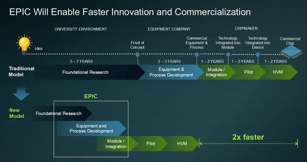
Representing a roughly US $5 billion investment, EPIC is the largest commitment to advanced semiconductor equipment R&D in U.S. history. When it opens in 2026, it will deliver state‑of‑the‑art cleanroom capabilities built from the ground up to shorten the path from early‑stage research to full‑scale manufacturing. But the facilities are only one component of the model. EPIC is also a platform, an operating system for high-velocity co‑innovation that revolutionizes how ideas move from the lab to the fab.

Advertisement

Diagram comparing traditional and EPIC chip innovation timelines showing 2x faster path EPIC is a platform, an operating system for high-velocity co‑innovation that revolutionizes how ideas move from the lab to the fab.Applied Materials

The EPIC model compresses the traditional workflow. Customer engineers work side‑by‑side with Applied technologists from day one — moving beyond isolated process optimization and downstream handoffs. Within a shared, secure environment, EPIC tightly integrates atomistic modeling, test vehicles, process development, validation, and metrology feedback. Constraints that once surfaced late in development are identified and addressed early.

The result is a potentially 2x faster path that benefits the entire ecosystem under one roof:

  • Chipmakers gain earlier access to Applied’s R&D portfolio, faster learning cycles, and accelerated transfer of next‑generation technologies into high‑volume manufacturing.
  • Ecosystem partners gain earlier access to advanced manufacturing technology and collaboration opportunities that expand what is possible through materials innovation.
  • Academic institutions gain opportunities to strengthen the lab‑to‑fab pipeline and help develop future semiconductor talent.

Building on decades of co‑development, we are reinventing the innovation pipeline with our partners across logic, memory, and advanced packaging to deliver the next leap in energy‑efficient AI.

Accelerating Advanced Logic

Logic remains the engine of AI compute. In the angstrom era, however, system‑level gains are increasingly constrained by power and energy. Extending AI performance now depends on architectures that deliver more performance per watt — accelerating the move to 3D devices such as gate‑all‑around (GAA) transistors, which boost density within a compact footprint while preserving power efficiency.

These architectural shifts are unfolding at unprecedented scale, with the logic roadmap already extending beyond first‑generation GAA toward more advanced designs. One key example is GAA with backside power delivery, which relocates thick power lines to the backside of the wafer, reducing resistive losses and freeing front‑side routing for tighter logic cell integration. Another example brings adjacent GAA PMOS and NMOS transistors closer together while inserting a dielectric isolation wall between them to minimize electrical interference. Further out, complementary FETs (CFETs) push density scaling even more by stacking PMOS and NMOS devices directly atop one another.

Advertisement

While these architectures deliver compelling gains in performance per watt and logic density without relying solely on tighter lithography, they significantly raise integration complexity. Manufacturing a single GAA device today can involve more than 2,000 tightly interdependent process steps. At the same time, wiring stacks continue to grow taller and denser to connect these advanced logic devices. Modern leading‑edge GPUs now in development pack more than 300 billion transistors into an area little larger than a postage stamp, interconnected by over 2,000 miles of wiring.

At this level of complexity, the process steps used to create these precise 3D devices and wiring stacks cannot be optimized independently. Design and process must evolve in lockstep, and materials innovation and fabrication methods must advance alongside device architecture. EPIC’s co‑innovation model is designed to accelerate exactly this convergence — enabling logic compute to continue advancing the frontiers of AI at the pace the roadmap demands.

Powering the Memory Roadmap

At the same time, the AI computing era is fundamentally reshaping how data is generated, moved, and processed — making memory technologies, especially DRAM, central to delivering the energy‑efficient performance AI systems require. As models grow larger and more data‑hungry, the DRAM roadmap is shifting toward architectures that deliver higher density, greater bandwidth, and faster access per watt.

At the DRAM cell level, this shift is driving a transition from 6F² buried‑channel array transistors (BCAT) to more compact 4F² architectures, which orient the transistor vertically to boost density and reduce chip area. Looking beyond 4F², sustaining gains in performance per watt will require moving past what 2D scaling alone can deliver. The industry is therefore turning to 3D DRAM, stacking memory cells vertically to add capacity within a constrained footprint. As these structures grow taller and aspect ratios intensify, high-mobility materials engineering in three dimensions becomes increasingly critical to performance and reliability.

Advertisement

Beyond the memory cell array, another powerful lever for DRAM scaling is shrinking the peripheral circuitry, which includes logic transistors and interconnect wiring. One emerging approach places select periphery functions beneath the DRAM array by bonding two wafers — one optimized for the DRAM cells and the other for CMOS logic — using multiple wiring layers.

In parallel, DRAM performance is being extended by leveraging logic‑proven enhancers in the memory periphery. These include mobility boosters such as embedded silicon germanium and stress films, along with wiring upgrades like improved low‑k dielectrics and advanced copper interconnects. Memory manufacturers are also transitioning periphery transistors from planar devices to FinFET architectures, following the logic roadmap to further improve I/O speed. These valuable inflections are central to EPIC’s mission — where they can be co-developed and rapidly validated for next‑generation memory systems.

Driving System Scaling With Advanced Packaging

As data movement becomes the dominant energy cost in AI systems, advanced packaging has emerged as a critical lever for improving system‑level efficiency—shortening interconnect distances, increasing bandwidth density, and reducing the power required to move data between logic and memory.

High‑bandwidth memory (HBM) marks a major inflection along this path. By stacking DRAM dies — scaling to 16 layers and beyond — and placing memory much closer to the processor, HBM enables rapid access to ever‑larger working datasets. This delivers step‑function gains in both bandwidth and energy efficiency.

Advertisement

More broadly, the rise of 3D packages such as HBM underscores why advanced packaging is becoming central to the AI era. Packaging now addresses system‑level constraints that logic and memory device scaling alone can no longer overcome. It also enables a move away from monolithic systems‑on‑chip toward chiplet‑based architectures, as AI workloads increasingly demand flexible designs that combine logic, memory, and specialized accelerators optimized for specific tasks.

A vital technology powering this roadmap is hybrid bonding. With interconnect pitches approaching those of on‑chip wiring, conventional bumps and microbumps run into fundamental limits in density, power, and signal integrity. Hybrid bonding removes these barriers by allowing dramatically higher interconnect and I/O density, supporting a broad range of chiplet architectures — from memory stacking to tighter compute‑memory integration.

As bonded structures like HBM stacks grow larger and more complex, warpage control, die placement, stack alignment, and thermal management become first‑order challenges. EPIC tackles these and other high‑value advanced‑packaging challenges through early, parallel co‑innovation across materials, integration, and manufacturing.

Bringing It All Together

Across logic, memory, and advanced packaging, our industry faces an ambitious roadmap that promises significant gains in energy efficiency for AI systems. But realizing that potential demands breakthrough materials innovation at a time when feature sizes are shrinking, interfaces are multiplying, and process interdependencies are escalating. These challenges cannot be solved on 10–15‑year timelines under the traditional relay‑race model. We must break down silos, align earlier across the ecosystem, and parallelize learning to keep pace with AI’s demands.

Advertisement

In the AI era, progress will be defined by the speed at which lightbulb moments turn into manufacturing and commercialization reality. The only viable path forward is a new innovation model — and EPIC is how we are driving it.

Source link

Continue Reading

Tech

Ireland and Northern Ireland share strong skill commonalities, finds research

Published

on

The Skills Insight Note is the first in the EGFSN’s Skills Insights series for 2026.

The Expert Group on Future Skills Needs (EGFSN) recently published a new ‘Skills Insight Note’ titled Cross Border Skills and Commonalities between Ireland and Northern Ireland. The research explores the labour markets of both Northern Ireland and the Republic of Ireland, with a particular focus on cross‑border workers, sectoral employment trends, education profiles and shared skills priorities.

The research – the first in the EGFSN’s Skills Insights series for 2026 – identified strong similarities between the Republic of Ireland and Northern Ireland, including a continued reliance on critical sectors, such as manufacturing, health and education, and a shared policy focus on future‑oriented skills in areas such as digitalisation, the green economy and apprenticeships.

Welcoming the data, Minister for Enterprise, Tourism and Employment Peter Burke, TD noted the importance of gaining insight into how both jurisdictions can cooperate effectively. 

Advertisement

“This Skills Insight Note provides valuable analysis of the labour market links and shared challenges between Ireland and Northern Ireland. The findings underline the importance of collaboration in skills development, particularly as both economies adapt to technological and demographic change. 

“Understanding these cross‑border dynamics strengthens our ability to plan effectively for enterprise growth, employment and long‑term competitiveness.”

Commuting figures, particularly from Northern Ireland to the Republic, were also found to have grown significantly over the course of the last 10 years. The research stated that this is reflective of labour market opportunities and shared economic strengths.

Minister of State with special responsibility for Trade Promotion, AI and Digital Transformation Niamh Smyth, TD said: “The findings clearly demonstrate the strong links that exist across the two jurisdictions, including shared skills priorities, sectoral strengths and growing levels of cross‑border commuting.

Advertisement

“This research highlights how closely connected our labour markets are and the opportunities that exist to address shared skills challenges through cooperation and coordinated policy approaches.”

Late last year, a new €9.85m cross-border project aiming to address critical public health challenges was launched in Belfast. The four-year OneHealth project is a health and life sciences partnership that will use AI and digital health approaches to tackle pressing health and agrifood challenges.

The initiative is being led by science and technology hub Catalyst in partnership with Atlantic Technology University, Queen’s University Belfast, Health Innovation Research Alliance Northern Ireland, Tyndall National Institute Cork and the University of Galway.

Don’t miss out on the knowledge you need to succeed. Sign up for the Daily Brief, Silicon Republic’s digest of need-to-know sci-tech news.

Advertisement

Source link

Continue Reading

Tech

IEEE Society ‘s Pitch Sessions Link Lab With Market

Published

on

The IEEE Communications Society (ComSoc)’s Research Collaboration Pitch Session initiative is proving to be a catalyst for meaningful engagement between academic researchers and industry innovators. Launched last year, the program connects promising researchers with industry leaders who can offer them funding, mentorship, and connections to bring interesting ideas closer to real-world deployment.

Rather than relying on chance encounters at conferences, the pitch sessions create a focused environment. Five academic presenters share their work with five industry representatives, known as “innovation scouts”: senior leaders primarily chosen from ComSoc’s Corporate Program partner companies such as Ericsson, Intel, Keysight, and Nokia. The curated format ensures that each idea receives dedicated attention from professionals who are seeking new concepts aligned with their organization’s priorities.

The initiative was launched in November at the IEEE Middle East Conference on Communications and Networking (MECOM) in Cairo and appeared in December at the IEEE Global Communications Conference (GLOBECOM) in Taipei, Taiwan.

AI-driven communication network

One of the most compelling outcomes came from the inaugural session in Cairo. Angela Waithaka, a student member and biomedical engineering student at Kenyatta University, in Nairobi, Kenya, presented her “AI-Driven Predictive Communication Networks for Enhanced Performance in Resource-Constrained Environments” paper. You can view her presentation along with others on IEEE.tv.

Advertisement

Waithaka’s research tackles a critical challenge: Next-generation communication systems increasingly rely on artificial intelligence and machine learning, yet most existing architectures consume abundant computational and energy resources, which are not always present in developing regions.

Waithaka proposed lightweight, adaptive AI/machine learning models capable of delivering predictive, reliable communication performance even under tight resource constraints.

Her vision resonated with Ruiqi “Richie” Liu, a master researcher at ZTE in China. ZTE is a global leader in integrated information and communication technology solutions. Liu says he recognized the relevance Waithaka’s proposal had to his company’s work with the International Telecommunication Union. He invited her to establish an ITU account so she could participate in the organization’s meetings discussing global telecommunications standardization projects—which would elevate her work to an international stage.

Simplifying data center protocols

The momentum continued at GLOBECOM. Among the presenters was Nirmala Shenoy, a professor at the Rochester Institute of Technology, in New York. Shenoy, an IEEE member, spoke on the topic of simplifying data center network protocols. She highlighted the growing complexity of the critical networks, which underpin cloud services, enterprise IT, and emerging AI workloads.

Advertisement

Shenoy’s focus on reducing protocol complexity while maintaining scalability, resilience, and low latency caught the attention of an innovation scout from Nokia, who heads its eXtended Reality Lab in Madrid. He found the key person at Nokia for Shenoy to connect with to discuss her research, and it led her to record a video for the company detailing her approach and its potential applications.

A model for accelerating innovation

The early success stories demonstrate the power of intentional, structured engagement. By bringing researchers and industry leaders together in a format designed for discovery, ComSoc is helping accelerate innovation and expand opportunities for collaboration. The pitch sessions are not merely conference events; they are becoming a bridge between academic creativity and industry implementation.

This year sessions will be held during the IEEE International Conference on Communications in Glasgow from 24 to 28 May, and more are scheduled during the IEEE International Mediterranean Conference on Communications and Networking in Sardinia from 6 to 9 July, and at GLOBECOM in Macau from 7 to 11 December.

As the program continues to grow, it could become a signature ComSoc initiative, one that strengthens the research ecosystem, supports emerging talent, and ensures that promising ideas find pathways to real-world impact.

Advertisement

From Your Site Articles

Related Articles Around the Web

Source link

Advertisement
Continue Reading

Trending

Copyright © 2025