Connect with us
DAPA Banner
DAPA Coin
DAPA
COIN PAYMENT ASSET
PRIVACY · BLOCKDAG · HOMOMORPHIC ENCRYPTION · RUST
ElGamal Encrypted MINE DAPA
🚫 GENESIS SOLD OUT
DAPAPAY COMING

Tech

AI Learns the “Dark Art” of RFIC Design

Published

on

Summary

  • RFIC design is a complex “dark art” that limits progress in wireless technologies like 5G, autonomous vehicles, and satellite communications.
  • Princeton researchers use reinforcement learning and inverse design to rapidly create RFICs from scratch.
  • Diffusion models rapidly generate novel or human-interpretable RF layouts, achieving record performance and drastically reducing design time.
  • Future progress needs large, shared chip design datasets and open ecosystems so AI can learn universal electromagnetic and circuit behaviors.

Take a moment and try to imagine your life without the wireless advances of the past three decades.

Have you lost your luggage? What a shame AirTags have not been invented. The airline representative has promised to call with updates, so settle in for a long wait by the kitchen telephone, because there are no affordable cellphones. You’ll be stuck listening to whatever is on the radio while you wait, because there are no streaming services. That’s not even to speak of all the movie plots that would have been ruined.

This is just a tiny sliver of how wireless technology makes itself felt in your day-to-day existence. The effects it has had on supply chains, infrastructure, and how the economy runs have been world-altering.

None of it would be possible without the radio-frequency integrated circuits that allow all our devices to unobtrusively send and receive information.

Advertisement

Now imagine what the further evolution of this technology will bring: Wide-spread autonomous vehicles, quantum communications, 6G mobile service and satellite communications. Continued momentum will depend on newer and more advanced versions of today’s RF chips.

But there’s the rub. Whereas the design of most of the world’s computing chips has been standardized into its own science, RF design has remained stubbornly in the realm of art. A dark art, even, that is mastered only through years of experience. As any sorcerer will tell you, the dark arts keep their own schedule. And that schedule is impeding progress not just in RF chip design but in every other technology that depends on it.

About seven years ago, in the wake of AlphaGo’s victory over world Go champion Lee Sedol, my students at Princeton and I began to wonder: Could AI be taught this art as well? Recent successes suggest that, to a large extent, it can. Over the last few years, our group and other leaders in the field have started to develop machine-learning-driven algorithmic methods for designing RFICs. Some of the resulting chips look more like modern art than circuit layouts. Yet in many cases, the physical prototypes bested state-of-the art circuits in terms of performance. The real achievement, however, is that it took the AI orders of magnitude less time to conceive a working design than it would a human designer.

This is not about one or two RF chips. AI-enabled design could be the future of all RF design, and maybe much more.

Advertisement

The Dark Art of RFIC Design

So why do these chips all have to be crafted by hand? Why aren’t RFICs designed with an algorithmic synthesis process, much as CPUs and GPUs are?

The design of RFICs is an exercise in engineering across multiple physical domains. Maxwell’s equations, operating across different spatial and temporal scales, govern how electromagnetic fields interact with active and passive devices that must be carefully codesigned for the chip to function. Alongside these are the laws of thermodynamics, which determine how heat is generated and removed during operation, as well as the mechanics of thermal expansion and contraction that dictate how reliably the chip and its packaging survive temperature changes.

Simultaneously accounting for all the physical constraints these impose makes the design space almost impossibly large. Every decision involves complex priorities that often compete with one another, preventing the optimization of any of them.

To better understand the issue, let’s walk through the steps involved, after which you’ll better understand why a single new chip design takes years and tens to hundreds of millions of dollars.

Advertisement

Colorful close-up of a microchip die showing intricate circuits and connection pads

Close-up of a glowing gold microchip circuit with dense patterned components.

Close-up of a microchip die with intricate golden circuit patterns and pads.

Close-up of a patterned microchip die with intricate gold circuitry on a dark background

Close-up of an intricate gold microchip circuit pattern on a dark background

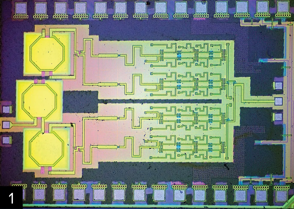
Microscope view of intricate gold microchip circuitry with numbered frame \u201c6\u201d.Most of the area of radio-frequency integrated circuits is dominated by complex electromagnetic structures. Human-designed RFICs, like this broadband power amplifier [1], start with templates and follow a symmetric, understandable pattern. But freed from the constraints of human-designed templates and the need for humans to even understand the rationale of electromagnetic structures, power amplifier ICs [2–5] and low-noise amplifiers [6] can take on truly wild-looking yet efficient designs. SENGUPTA LAB

Let’s say you’re an engineer assigned to design a new 28-gigahertz power amplifier for a 5G-millimeter-wave handset. (This is the type of RFIC that boosts the 5G signals on your phone and transmits them to the antenna where they can be picked up by a distant base station). Where do you start?

RFIC design has some features in common with house building. Just as the blueprint for a house dictates the number of bedrooms and bathrooms to be built and the hallways connecting them, the blueprint for an RFIC—called the architecture—establishes the kinds of elements the RFIC needs to fulfill its intended function. Instead of rooms, the architecture includes, for example, the number of stages of amplification your power amplifier needs. Instead of hallways, it shows the paths that signals must take to get through those stages.

The blueprint for RFICs is actually mostly hallway; passive elements, like inductors and transmission lines, take up far more real estate than active elements like transistors.

Here’s why. As you have probably experienced yourself, a typical CPU’s transistors overheat when faced with operating frequencies of just a few gigahertz. The frequencies RFICs can operate at are higher by an order of magnitude—28 and 39 GHz for 5G signals, 26.5 to 40 GHz and even higher for satellite communications, and 77 GHz for automotive radar. Under this onslaught, a CPU’s transistors would fail.

Advertisement

RFIC transistors avoid this fate because these chips cleverly manage the signal’s energy with careful electromagnetic design. This takes the form of byzantine networks of metal elements that dominate the chip’s real estate. These structures are geometrically regular, often symmetrical, and so intricately constructed they sometimes resemble lacelike filigree. But while they may look decorative, they are essential to the chip’s functioning.

Electrically speaking, these “hallways” work more like the chip’s plumbing. Like plumbing, this extensive labyrinth of passives confines electromagnetic energy only to the places it should be traveling around the chip.

The major challenge in RFIC design is putting all these elements together to ensure they work, just as constructing a house from its blueprints demands exact specs for load-bearing beams, pipes, and external walls. On an RFIC, the architecture needs to be realized with physically fabricable transistors and passive components that are connected just so, to permit the signal to travel through the chip and be processed. The way these devices are connected locally is what we call the circuit’s topology.

The RFIC Design Process

To make that power amplifier, then, your first step is to identify a candidate circuit template: The combination of structures that will meet the goals of a particular architecture with a specific circuit topology. Over the years, researchers have eased your burden by developing reusable design templates for specific functions. For example, templates suggest how many amplification stages a circuit needs (because sometimes, combining the output of two smaller amplifiers will result in better bandwidth and efficiency than you would get from a single larger one). And they suggest what the general configuration of the passive structures should be. Today there is an extensive library of such templates.

Advertisement

However, these can’t simply be used off-the-shelf, because each comes with trade-offs. Some have better gain at the expense of stability; some better bandwidth at the expense of efficiency; still others are more energy efficient at the expense of output power, and so on. There is rarely a clear best choice.

To arrive at the “sweet spot” where all these different parameters are balanced into optimal harmony, designers will typically lay out several different versions of the circuit, using intuitions and methods they have picked up in their years of training.

The challenge is that the decision around the architecture, circuit topology, or the electromagnetic passives cannot be done separately. One decision influences the others. So, designing an RF circuit can often feel like trying to fit an oversized carpet into too small a room—press down one corner, and another pops up.

At microwave and millimeter-wave frequencies, even the smallest misstep is the difference between a chip that works and one that doesn’t, and any number of things can go wrong. For example, when an electromagnetic wave encounters a transistor—or any other component —the path it travels must be properly “matched” to what comes next. If it isn’t, some of the energy reflects backward instead of flowing forward. Imagine trying to connect a high-pressure fire hose directly to a narrow garden hose. Without the right adapter, water will splash backward at the junction. Very little will make it through. In electronics, this is called the impedance-matching problem.

Advertisement

To prevent those reflections, engineers design special transitions, essentially microscopic adapters, that smooth the handoff between components. On a chip, these adapters can be surprisingly intricate. They don’t just pass the signal along; they can also split it, combine it, or distribute it across multiple paths with carefully controlled timing and strength.

Once you’ve done the architecture, plumbing, and everything in between comes the moment of truth. Have all the choices you have navigated through the enormous design space resulted in an RFIC that meets its specifications? If the specifications are not met, you will have to go back, either redoing the topology or the entire architecture, and repeat the whole process. So get ready for months of time- and resource-heavy simulation and iteration. Perhaps you now see why, for decades, a core belief has persisted in the RFIC community: “RF design is an art.” It was said that only an experienced designer—with an artisanal understanding of how the pieces make up the whole—could master the subtleties of analog and RF design. Unfortunately, this entrenched notion has long held back algorithmic innovations in the field just when we need them most. Traditional, artisanal RFIC design is hitting its limits as the complexity of these systems inexorably grows.

AI for RFIC Design

While RFIC designers continued their battle against their “oversized carpet” problem, a series of interesting developments emerged in allied disciplines. Across a range of other previously intractable problems like protein folding and climate modeling, AI has been able to successfully navigate multidimensional complex spaces. This gave us the incentive to look deeper into AI for RF. After all, the combinatorial complexity of protein folding is not that different from the nature of the design space in our domain.

We were not the first to think of using artificial intelligence to speed up parts of RFIC design. Researchers had previously trained machine learning algorithms on circuit templates in the hope of speeding up the normal optimization processes. While this approach was undoubtedly faster than humans at optimizing templates, it still relied fundamentally on libraries of existing designs invented by humans.

Advertisement

We didn’t want that. We wanted to break free from the restrictions of prefabricated topologies. Because while a designer’s experience and hard-won heuristics are crucial to building a working design, they also place fundamental limits on it. Furthermore, such an approach would necessarily require simulation steps as part of the optimization cycle, and even the fastest simulations use a lot of computing resources. Worse still, in many advanced cases, such as for broadband designs, there are no existing templates.

But if we didn’t start with templates, where could we start?

The goal here was to allow algorithms to determine—entirely from scratch—every parameter for architecture, constituent circuits, and electromagnetic passives. This approach differs fundamentally from conventional optimization, which is limited to determining the parameters—like transistor dimensions and passive component geometries—that optimize structures originally devised by humans.

In our new approach, the architecture begins essentially from nothing and is progressively assembled through successive iterations. The system explores the design space by generating myriad candidate circuit combinations and mapping the resulting performance trade-offs as it navigates this landscape. Because the process is not biased by prior human design choices, it can produce completely novel circuit topologies that look markedly different from those created by human designers.

Advertisement

In some ways, the approach echoes AI systems such as AlphaGo Zero, which achieved superhuman performance not because it was trained on games played by humans but because it explored the rules by playing against itself. Similarly, our algorithm develops new circuit architectures by exploring and evaluating its own design strategies. In so doing, it learns to understand circuits, electromagnetics, and the close codesign they need to achieve the end-to-end design of RFIC.

Inverse Design for RFICs

To realize this capability, we proceeded in two stages. First, we developed a reinforcement-learning (RL) framework that determines the optimal system architecture, circuit topology, device parameters, and even the properties of the electromagnetic interfaces that connect different circuit elements. In this stage, the algorithm effectively defines how signals should propagate and interact across the system.

The algorithm trains very similarly to how a computer learns to play a game. If you let it play enough times, it can learn to play better by observing the relationship between the actions it took and the score it achieves. In a similar way, the RL agent here learns to design effective circuits by playing with a set of combinations, and over time, it can map the space between the circuit performance to its architecture, topology, and parameters. This training takes a few days to a week, but once trained, the agent can design circuits very quickly

The next step was to determine the physical structure of the IC’s electromagnetics—the plumbing—that can create the desired properties of the passive elements, which are characterized by a set of metrics called scattering parameters. These measure if a signal entering a component actually moves forward—or is reflecting backward, being wasted, as in our previous example with the fire hose and the garden hose.

Advertisement

Deriving the structure from the desired scattering parameters is an example of an approach called inverse design, which appears across many areas of engineering. In structural engineering, for example, one might collaborate with an architect on a physical goal—such as creating large interior spaces with high ceilings—and then determine the arrangement of arches or buttresses that can support it.

Generative AI for Electromagnetic Networks

Diagram linking S-parameter curves to classical, mazelike, and pixelated structures.
In an effort to make AI-designed circuits more understandable, engineers took a page from image-generation AIs that allow users to create pictures in the style of different artists. Here, instead of an artist\u2019s style, the user can dial in the spatial frequency of an electromagnetic structure. Regardless of how pixelated the structure is, it will still reproduce the needed electromagnetic characteristics, or S-parameters.
Chris Philpot

But RF integrated crcuits pose a particular challenge for inverse design: The process must account simultaneously for circuit behavior and the electromagnetic responses of the interconnects and passive elements that link them together. But it has to figure that out without doing a lot of artisanal iterating.

So we replaced our RF circuit simulator with an AI-based emulator. This AI model can predict the behavior of electromagnetic fields going through any structure—even totally arbitrary two-dimensional shapes—without having to compute the underlying physics from scratch, as simulation tools do. It would predict the solution of Maxwell’s equations and tell you the scattering parameters for any structure you showed it, without actually doing the math. With such an AI in hand, what a time-consuming electromagnetic solver normally takes minutes or hours to accomplish is reduced to milliseconds.

Advertisement

We chose to build our emulator around a convolutional neural network—a machine learning model that has been remarkably successful for image processing. Such networks can extract spatial features from any structure, and it turns out that the image of a structure contains a lot of spatial information that can accurately predict its electromagnetic performance. Then we trained it on a vast number of random pixelated structures whose scattering parameters had been labeled.

Once we had our inverse-design RL and suitable AI emulator, we essentially had an end-to-end AI designer. So we asked it to design us a power amplifier.

Unconventional RF Architectures

In 2023, we published this proof of concept—a power amplifier targeting the millimeter-wave band, specifically spanning 30 to 100 GHz, which covers most of the relevant 5G and radar frequencies. The final design achieved the best combination of wide bandwidth, output power, and efficiency then reported for a silicon-based power amplifier—meaning it could amplify a large amount of data across a wide swath of frequencies—while maintaining record efficiency.

The structure of the IC’s electromagnetic pathways was unlike anything any human would ever consider. Since the AI is not trained on human designs, the layout that emerged looked more like an arbitrary pattern or perhaps a QR code than the regular symmetrical structures we are used to seeing.

Advertisement

One unexpected insight revealed by this prototype, and our research generally, is that there’s no evidence that the templates we’ve historically relied on are even close to optimal for modern design goals. It’s not that a human designer can never come up with a better design. But with the removal of the templates and the time to synthesize cycle upon cycle of optimized circuits, it is now clear that AI-driven synthesis could break traditional design barriers and push the limits of RFIC capabilities.

Our 5G amplifier had only one input port and one output port. Adding more inputs and outputs to a design is not straightforward. Every port electromagnetically couples to every other port, so the scattering parameters quickly add up. Two ports give you four scattering parameters. Four ports, 16 scattering parameters. The math gets ugly fast. Could our model keep up?

We next trained our model on larger classes of electromagnetic structures with many input and output ports. In 2024, we published work showing that multiport integrated circuits are no problem for these AI algorithms either. Where previously multiport electromagnetic simulation required days or weeks of toil, this model evolved new structures in minutes. Since then, a plethora of work in the space by research communities across the globe have demonstrated the power of inverse design in RFIC.

Combining the reinforcement learning framework with the inverse design, we now had the ability to create an RFIC from specifications all the way to a fabrication-ready layout. We’ve so far shown this is true for RFICs ranging from low-noise amplifiers to subterahertz and broadband power amplifiers. The hope is that this will work just as well for other circuits.

Advertisement

Making AI Designs Interpretable

Our goal was to make RFIC design better and easier, but we didn’t want to make it beyond human understanding. Chip testing and debugging is a long, arduous process, sometimes even more so than design. Engineers often prefer ICs to have interpretable structures, so that if a problem crops up, they can understand how the chip works well enough to debug it.

To create structures that are more interpretable, we turned to diffusion models, which you may know from their remarkable ability to generate realistic images from text prompts.

AI-driven synthesis could break traditional design barriers and push the limits of RFIC capabilities.

Imagine you go to your favorite image-generation engine and ask it to create a painting of the sky in the style of Picasso, Van Gogh, or Michelangelo. You will get images that capture the essence of their brushstrokes, their use of colors, and their framing. All are pictures of the sky nonetheless, but in different styles.

Advertisement

Electromagnetic design is similar in that multiple structures can have very similar electromagnetic responses. Instead of using text input, we used scattering parameters as our input, and the electromagnetic structure of an RFIC chip as our output. As part of the inputs to the diffusion model, we created a dial that sets the spatial frequency of the final structure. By turning the dial, a designer can direct the model to synthesize structures with low (classical-looking and interpretable), medium (mazelike structures), or high (pixelated or arbitrarily-shaped) spatial frequency.

From prompts to output, the entire process took about 6 minutes. With this diffusion model, algorithms can now both discover novel architectures and accelerate the creation of conventional, so-called classical ones.

All an RFIC designer needs to do is specify virtually any valid set of scattering parameters. As long as they are physically realizable under Maxwell’s equations, the model pops out a corresponding structure as if it were a vending machine.

The Future of AI-Driven RFIC Design

The results of our investigations have drawn the attention of the RF community. The traditional bottom-up design process is clearly beginning to reverse.

Advertisement

But there are still questions: How generalizable are these methods? Can they consistently deliver truly high performance? Can we get to a place where AI produces designs that maximize every conceivable trade-off, holistically optimizing every parameter to its most ideal physical state? We want to take this strategy beyond RFIC design and invent other kinds of circuits that are different from anything humans have ever done.

These are exciting and ambitious prospects, but we are not there yet. AI can hallucinate a design that creates bad circuits that don’t work. This means verification methods need to remain under human oversight. And, while hallucinations are rare, it would still be good to reduce their occurrence.

History suggests that meeting these dreams of the future will take much more data than we’ve been using. Before the creation of the ImageNet repository—a repository of 14 million varied, human-annotated images—image-recognition models didn’t function well in the real world. The datasets they had been trained on were too tiny to be effective. ImageNet’s massive amounts of training data ushered in a revolution that led to AI that can generalize and recognize images in the wild. The rest was history.

If the goal for RFIC and analog design is a universal foundational model—something that learns the governing laws of electromagnetics and circuit behavior—then we also need data.

Advertisement

The good news is that this data is plentiful. Around the world, countless engineers at companies and academic labs simulate nearly identical RF circuits and passive structures every day. The bad news is that it’s all locked away behind nondisclosure agreements.

Open ecosystems have propelled other areas, and we think the RFIC community should do the same. There had been some movement toward this. Natcast, the operator of the U.S. CHIPS and Science Act’s R&D program, would have bolstered shared infrastructure and innovation for the next generation of wireless, sensing, and defense technologies. Unfortunately, both the organization and the program it ran specifically for machine learning and RFICs have been closed.

But the momentum Natcast’s effort sparked hasn’t died out. Building on our early work, groups across the community have already demonstrated remarkable advances. AI-driven IC design is part of a much broader technological shift. From biology and materials science to automotive and aerospace engineering, AI is reshaping how complex systems are conceived and optimized. Deeper collaboration between AI researchers and chip designers will unlock the field’s full potential. It’s by no means a foregone conclusion, but if we get this right, this genie won’t stay in its bottle.

From Your Site Articles

Advertisement

Related Articles Around the Web

Source link

Advertisement
Continue Reading
Click to comment

You must be logged in to post a comment Login

Leave a Reply

Tech

What a Restored Nikon Microscope Showed Inside a 1980s Motorola Microcontroller

Published

on

1980s Motorola Microcontroller Up-Close Microscope
A single chip bought on a whim during a late-night scroll turned into an excuse to rescue an old laboratory microscope and finally see what its silicon actually contains. The part in question is a Motorola MC68701, a microcontroller built in the early 1980s. It packs an enhanced 6800-family processor, 2 kilobytes of ultraviolet-erasable program memory, 128 bytes of RAM, a serial interface, a programmable timer, and 29 input/output lines all onto one piece of silicon. In its day that counted as a complete small computer in a single package, and it could even reach out to external memory to grow beyond its on-chip limits.


The chip’s ceramic container contains a small quartz window that directly covers the silicon. That window exists so that UV radiation can wipe the program memory as needed. It also allows anyone with the proper optics to see the die without having to open the packaging or use harsh chemicals. That feature was what made the entire endeavor possible.

Sale


Motorola Moto G Stylus – 2025 | Unlocked | Made for US 8/256GB | 50MP Camera | Pantone Gibraltar Sea
  • Unlocked: Compatible with all major U.S. carriers, including Verizon, AT&T, T-Mobile and other major carriers.
  • Premium built-in stylus. Effortlessly jot notes, edit photos, sketch artwork, and navigate on the only phone in its class with a built-in stylus***.
  • Striking design with advanced protection. Make a statement with an ultrathin design, modern colors, and a vegan leather finish plus outstanding water…

The person who ended up with the chip realized that a simple microscope would suffice to begin exploring. An affordable Nikon Labophot trinocular model appeared on eBay, complete with the original lighting system but in poor condition. Bringing it back to working order required numerous procedures. The power supply required maintenance since a transformer had become loose within its housing. Once fastened and tested, the optics were meticulously cleaned with high-purity alcohol and soft swabs to eliminate decades of dust and haze. A flexible LED light source was added to the top for reflected illumination, and a standard microscope camera required a special adapter manufactured on a small CNC mill to fit firmly over one of the eyepiece tubes.

Advertisement

1980s Motorola Microcontroller Up-Close Microscope
He placed the MC68701 under the microscope. Even at low magnification, the bond wires that connect the silicon to the package pins were visible; they were simply thin gold strands arching from tiny pads on the die’s edge to the chip’s legs. Moving on to the 4x objective (approximately 40x total when you include the eyepieces), you can see the surface details. The largest visible structure is the program memory array, which is a vast, regular grid that covers a large region, with each little compartment looking nearly identical to its neighbor. Not bad for read-only memory, which is designed to be dense and simple.

1980s Motorola Microcontroller Up-Close Microscope
There are line-driver transistors nearer the die’s edges, near the bond pads, because these are the circuits that generate the signals required to connect the device to the outside world. The transistor forms differ from the dense logic in the core, and faint squiggles of metal trace extend all the way up to the pads where the gold wires are connected. When you see those drivers in action, it becomes evident how the chip sends and receives information. Multiple layers of metal traces run over the surface, some horizontal, some vertical, and some on a higher plane, allowing signals to cross over without shorting. Even without delying the chip, you can see the stacking effect, demonstrating how meticulous they were in fitting everything into such a little space.

1980s Motorola Microcontroller Up-Close Microscope
Other functional blocks can be found elsewhere on the die. There are three components: one for instruction decoding, one for arithmetic and logic tasks, and a small piece for the on-chip RAM. None of these blocks required labeling because their sizes and locations indicated exactly what they were intended to perform. Once the microscope is focused, the entire active surface fits comfortably into the field of view, but all of the features are so small that you need steady illumination and a bit of care with the focus knob to discern the minute details.

Source link

Continue Reading

Tech

He Comes To Bury Segmented Memory, Not To Praise It

Published

on

[BillPg] has been designing a fantasy 1980s-era home computer. As part of the exercise, he’s reevaluating all the assumptions that have grown organically over time in the small computer landscape. Hindsight is, so they say, 20/20, but sometimes hindsight can also be colored by modern thinking. Sometimes an idea that seems stupid today made sense in the context of its time. In particular, [Bill] has thoughts on the much-maligned 8086 memory segments.

If you haven’t run into it before, the 8086/8088 had a problem. It wanted to be more or less conceptually software compatible with the 8080 and Z80 computers, which had 16-bit addresses, leading to a limit of 64K of memory. When Intel was designing the next generation of chips, it knew that 64K had to go, but telling developers that code would require huge reengineering was a non-starter. So the idea was to provide multiple 64K spaces broken up into segments.

As with most things, there is theory, and there is practice. In theory, a 16-bit segment provided four extra address bits to add to the existing 16-bit address, producing a 32-bit address, even though the CPU only had 20 bits of address bus. Code that fit in 64K could pretend like that was the whole world, and a tricked-out system could have 16 worlds. Future systems could, in theory, have had more.

In practice, Intel made the segment the top 16 bits of a 32-bit address and then added it to the ordinary 16-bit address. So address 0000:0010 (segment=0, address=10 hex) is the same memory location as 0001:0000. Address 0010:0010 is the same as address 0000:0110 and 0001:0100. This wasn’t really the intent, just a byproduct of how the chip worked.

Advertisement

Eventually, the segments would become indices into a table (like the title graphic), but by then, bad practices wiped out a good idea. It is doubtful that the original designers thought anyone would take advantage of the overlapping address, but, of course, they did.

By the time the 80286 and beyond produced segments that were really keys which defined a block of memory, everyone was already in the mode of using the segment and offset as a large pointer. C compilers even had “modes” that let you treat the segment as just more address bits. Because of that, even on newer processors, people had a tendency to build a “flat” segment and use it. That is, make a segment that starts at 0, ends at the end of memory, and then forget about segments.

In fact, many people independently discovered that you could define a flat segment in protected mode, return to real mode, and then enjoy a flat address space. This was later christened unreal mode, and a topic we’ve covered a few times before.

We agree with [Bill]. Segments were a good idea at the time and might have been more important if people had used them the “right” way. Of course, there would have been ups and downs. Proper segments might have allowed for easy virtual memory, for example. But at the price of possibly swapping in and out huge segments instead of relatively small pages. Today, most of what segments were supposed to do is part of the memory management unit and is mostly hidden from the application developer. Still, interesting to reflect on why Intel made that choice and how we got to where we are today.

Advertisement

Source link

Continue Reading

Tech

Home Broadband Is 5G’s Surprise Killer App

Published

on

5G telecommunications, according to industry hype when 5G first launched in 2019, was going to be all about buzzy applications like mobile augmented reality and autonomous vehicles. But the surprise plot twist came when replacing home cable internet turned into 5G’s most widely adopted new application.

Fixed wireless access (FWA) now serves over 14 million U.S. customers, and contributes 28 percent of worldwide wireless traffic. Fixed wireless access is what the term sounds like: broadband internet delivered over a cellular radio link to a stationary location—no cable, no fiber, no trenching, no satellite broadband antenna pointed at the sky. What makes FWA distinctive is that it repurposes the same towers, spectrum, and 5G infrastructure that was built for mobile devices.

One U.S. Federal Communications Commission commissioner has called FWA 5G’s killer app. And that’s true not just in the United States either. Jio, India’s largest carrier, is also one of the world’s largest FWA providers, with over 9 million customers as of last year.

Carriers discovered they could repurpose surplus 5G capacity, while also exploiting a usage pattern quirk: mobile traffic starts to drop after 8 p.m., just when home internet usage peaks. The result is broadband, delivered via traditional cellphone towers, at a lower cost than fiber deployment. For these reasons, FWA provides real price competition to cable broadband, while reaching underserved rural and suburban communities.

Advertisement

Fixed Wireless Access Repurposes Ambitious 5G Infrastructure

FWA is cheaper to deploy than fiber, and for most homes and small businesses, fiber’s gigabit speeds are overkill anyway. And since FWA uses the same wireless networks built for cellular service, FWA works anywhere that receives a steady cellular signal.

As cellular networks extend into areas with minimal service, FWA’s coverage map expands with them. In these remote locales, the other main viable broadband alternative typically comes from satellite services like Starlink—which are, compared to FWA, more expensive, with higher delays, and lower bandwidth.

While most FWA deployments use currently underused microwave bands, some FWA deployments use electromagnetic spectrum that 5G launched but that mostly failed with mobile users. Millimeter waves operate at frequencies 10 to 40 times higher than 4G’s spectrum, offering high data rates from their wide available bandwidth.

However, there are good reasons 5G mobile users today don’t generally use millimeter-wave spectrum. Millimeter waves can’t penetrate buildings. Plus, they lose signal strength within a kilometer or two of the transmitter. Millimeter-wave antennas are also a real drain on cellphone batteries compared to microwave and radio-wave tech.

Advertisement

Yet none of these challenges applies to a fixed station with a clear line of sight to a nearby tower. FWA home units (called customer premise equipment or CPEs) outperform 5G handsets by a significant margin. That’s mostly because of hardware. CPEs carry larger, more sensitive antennas than a typical cellphone, paired with more capable transceivers. CPEs also tend to be plugged into wall outlets, making battery concerns a nonissue.

Another 5G technology that did not gain traction in mobile wireless is multi-user multiple-input multiple-output (MU-MIMO). A base station with MU-MIMO uses an array of antennas to serve multiple users on the same frequency simultaneously.

However, maintaining a MU-MIMO signal involves tracking each user individually—a problem that quickly becomes overwhelming with enough mobile users. FWA is different, however. Static CPEs, with their steadier downlink traffic loads, are an ideal match for MU-MIMO technology.

So, FWA internet service not only uses mostly fallow spectrum but also uses 5G spectrum more efficiently than do 5G mobile users—for whom, of course, these 5G technologies were originally designed!

Advertisement

How FWA Became 5G’s Surprise Killer App

Not long ago, the high-bandwidth use cases for 5G made for an impressive list: millisecond latency for autonomous vehicles, mobile augmented reality headsets with extensive high-speed data needs, and massive machine connectivity for an expanding internet of things (IoT).

These applications have all stalled. Autonomous vehicles pose challenging—and still unsolved—problems unrelated to spectrum allocation. Augmented and virtual reality technologies have yet to create meaningful spikes in bandwidth demand. And the IoT has, to date at least, fragmented across an array of competing standards.

Mobile carriers had built dense 5G networks for mobile customers whose needs rarely saturated the network’s capacity. Home broadband usage peaks in the evening hours, precisely when cellular networks are quietest.

FWA sits at cellular networks’ crossroads of supply and demand.

Advertisement

The Advent of 6G Will Only Expand FWA’s Reach

In December, the telecom standards body, the Third Generation Partnership Project (3GPP), issued its latest 5G specification—Release 20, the final “5G only” update. So, although 6G is still years away (its first specifications are expected in early 2029), engineering decisions that will define 6G are being made today. And FWA is not on the margins of that conversation; FWA is currently considered an established day-one use case.

6G wireless technology promises to expand FWA’s reach—not only via spectrum but also via geometry. Instead of following 4G and 5G’s connectivity model—strong signals near towers and weak signals far away—future 6G networks will let homes connect to multiple towers simultaneously, using a technology called distributed MIMO (multiple-input, multiple-output).

Where 5G’s version of MIMO (a.k.a. massive MIMO) concentrates user communication with dozens of antennas at a single tower, distributed MIMO uses antennas across multiple base stations and coordinates them to deliver signals to your home from multiple directions simultaneously.

The practical result: Because no single tower is responsible for any given connection, the “edge” of a cell network—that outer boundary where signal strength falls off and service degrades—no longer represents a hard limit on who gets well served. A home that would once have been too distant from a tower, or blocked by terrain, could now be within reach of several base stations working together.

Advertisement

6G may eventually adopt distributed MIMO technology for mobile users, when synchronization challenges and other signal engineering hurdles are solved and deployed for real-world cellular networks. The jury, as of 2026, is still out on whether the full distributed MIMO problem will be solved once the 6G standards start to be set in place, within three years.

As demand for FWA grows, carriers will also deploy increasingly capable millimeter-wave infrastructure for fixed customers first—the stationary CPE use case that millimeter wave best suits. The dense millimeter-wave antenna infrastructure that FWA requires is the same infrastructure that future mobile applications will eventually inherit. AR glasses, AI-powered wearables, and other bandwidth-hungry applications originally promised for 5G are not canceledthey are waiting for the infrastructure to arrive.

The pathway to FWA is being prepared at lower frequencies, too. There is growing interest today in the largely unoccupied FR3 band, which spans roughly 7 to 24 gigahertz, situated between crowded low/mid-bands and the much higher millimeter-wave frequencies.

Recent field trials by Nokia have demonstrated FR3’s viability for both cellular and FWA applications. FR3 is emerging as one of the more promising near-term frontiers for extending FWA coverage beyond its current footprint.

Advertisement

None of this was the plan. No carrier executive in 2020 stood on a stage and announced that 5G’s defining achievement would be delivering living room broadband to rural homes and suburban subdivisions underserved by cable.

FWA became 5G’s killer app because the engineering economics made it happen. Surplus wireless capacity met unmet consumer broadband demand, with the physics of a stationary receiver doing the rest.

That is not a criticism of the engineers or the carriers. It is simply how technology sometimes advances—sideways, through gaps nobody was trying to fill.

But FWA’s model of prioritizing unconnected users may in the end prove to be telecom’s on-ramp to everything else. Fix the digital divide first. Tomorrow’s sci-fi future appears set to follow close behind.

Advertisement

From Your Site Articles

Related Articles Around the Web

Source link

Advertisement
Continue Reading

Tech

Tesla launches a longer six-seat Model Y to replace the Model X for many buyers

Published

on


Tesla has taken this approach before. Instead of launching brand-new cars, the EV giant has focused on new versions of the Model Y and Model 3 to support demand. Tesla rolled out the longer Model Y L in China last year, where it lifted sales even as local rivals like…
Read Entire Article
Source link

Continue Reading

Tech

Shampoo and cookies get an AI makeover as consumer giants rewire their labs

Published

on

The AI story has mostly been told through chips, data centres, and the companies building the models. It is now being told through the shampoo aisle.

The world’s largest makers of everyday goods, the businesses behind the bottles and packets in most kitchens and bathrooms, say they are using artificial intelligence to design products and run the campaigns that sell them, turning a technology associated with software into a fixture of the consumer-goods lab.

It is the same wave of enterprise adoption that has pulled AI tooling into corporate software stacks, arriving now in categories as unglamorous as body wash and biscuits.

Procter & Gamble offers the clearest example of what this looks like inside research and development.

Advertisement

The 💜 of EU tech

The latest rumblings from the EU tech scene, a story from our wise ol’ founder Boris, and some questionable AI art. It’s free, every week, in your inbox. Sign up now!

The company says it used AI to screen tens of thousands of peptides in developing a formula for a Pantene product, drawing on an internal database of more than 8,500 formulations to predict how a mixture would feel on skin or hair before anyone mixed it.

The point is not novelty for its own sake. It is time. Steps that once required rounds of physical testing can be narrowed down computationally, which pushes candidates toward consumer trials faster.

Advertisement

Mondelez, the snacking company behind a long list of familiar biscuit and chocolate brands, describes a similar shift on the food side.

It says an AI product-development tool has helped it generate dozens of new formulations, and that the software lets developers move between two and five times faster than conventional methods.

The same generative systems are being pointed at marketing, producing personalised images, text, and video at a pace traditional studios cannot match.

Unilever has leaned hardest into the campaign side. Its Dove brand ran a cookie-scented body-care line in partnership with Crumbl, with AI involved across the effort, from product direction to the selection of influencers and the creative itself.

Advertisement

The company reported the campaign drew billions of impressions and brought a large share of new buyers to the brand. Whatever one makes of a cookie-scented soap, the mechanics are instructive: a single AI-assisted pipeline running from formulation to feed.

What ties the examples together is compression. In consumer goods, the traditional cost of experimentation is measured in months of lab work and test batches, and the traditional cost of a campaign is measured in agency hours. AI attacks both.

Reformulation becomes a search problem over known ingredients, and content becomes something generated and varied on demand, an approach that mirrors the advertising ambitions on display when OpenAI pitched AI-made ads at Cannes.

The claims deserve some caution. Most of the specific figures come from the companies themselves, and consumer giants have every reason to present their AI programmes as further along than they are.

Advertisement

Product development still ends with human tasting panels and dermatological testing, and a formula an algorithm likes is not the same as one a shopper buys twice.

The industry’s own researchers have flagged that AI-generated marketing often drifts toward the generic, missing the brand-specific character that makes a campaign land.

Still, the direction is consistent across firms that rarely agree on much. The reallocation of enterprise budgets toward AI agents and tooling has become a general feature of large companies, from Tencent’s enterprise agents to the consumer-goods R&D described here, and the packaged-goods sector is not sitting it out.

For shoppers, the visible result will be mundane: more variants, faster refreshes, scents and textures that arrive and vanish more quickly than they used to.

Advertisement

The machinery behind the shelf is changing even where the products look the same. A bottle of shampoo is, increasingly, the output of a search.

Source link

Advertisement
Continue Reading

Tech

Samsung’s appliance workers plan a rally over the bonuses going to chip staff

Published

on

The workers who build Samsung’s phones, televisions, and washing machines are about to make their unhappiness visible.

Their union says several thousand of them will gather near the company’s Suwon headquarters on 16 July to protest the bonuses their colleagues in the chip division have won, a grievance that has been building since the semiconductor pay deal was struck in May. Somewhere between 2,000 and 3,000 people are expected to turn out.

The arithmetic behind the anger is easy to follow. Staff in Samsung’s Device eXperience division, the part of the company that makes the products most people actually touch, are set to receive a 2026 bonus of about 6 million won, roughly $3,900, paid in treasury shares.

Workers in the semiconductor division stand to collect up to 600 million won. That is a gap of about a hundred to one between two halves of the same employer, and it has proved impossible to explain away.

Advertisement

The 💜 of EU tech

The latest rumblings from the EU tech scene, a story from our wise ol’ founder Boris, and some questionable AI art. It’s free, every week, in your inbox. Sign up now!

The chip workers earned their windfall through a separate union and a separate negotiation, one that produced something unusual in Korean labour history.

Samsung agreed in writing to set aside a fixed slice of semiconductor operating profit, around 10.5 percent, for special bonuses, only the second time a major Korean company has put a percentage profit-share commitment into a binding contract.

Advertisement

For the people who negotiated it, that was a landmark. For everyone on the other side of the building, it looked like being written out of the story.

It is not hard to see why the semiconductor staff came away with so much. That division has been generating the overwhelming majority of Samsung’s profit, powered by the high-bandwidth memory chips that feed AI data centres, and the union pressed its advantage hard.

Chip workers had earlier been offered an average bonus of about $340,000 while threatening an 18-day strike that Samsung could not afford at the peak of a memory shortage. The leverage was real, and they used it.

The appliance and consumer-electronics workers have no such leverage, which is part of what the rally is meant to dramatise. Their division is profitable but ordinary, the kind of steady business that does not hold a company hostage.

Advertisement

The Donghaeng union, which represents the non-chip side, has already tried the legal route, going to court in Suwon to halt a companywide vote on the bonus arrangement. That effort did not stop the deal, and the demonstration is the next move.

What the protesters want is a revised allocation, one that treats the AI windfall as something the whole company earned rather than a prize belonging to a single division.

Samsung’s position has been that the chip bonus reflects the chip division’s contribution, a logic that is defensible on a spreadsheet and difficult to sell on a factory floor.

The dispute has also drawn wider attention, with policymakers flagging the scale of chip bonuses as a potential inflation risk in a country where Samsung’s payroll moves the numbers.

Advertisement

The rally itself is unlikely to change the 2026 payout, which is largely settled. Its purpose is to set the terms for the next round, and to remind Samsung that a two-tier workforce is a management problem as much as a budgeting one.

The company has said its special compensation package for chip staff exceeds industry norms, a claim that reads very differently depending on which building you work in. Record profits were supposed to be the easy part.

Whether the demonstration stays symbolic or hardens into something more disruptive will depend on what Samsung offers next.

For now, several thousand people who make the company’s most visible products are preparing to stand outside its headquarters and point out that they were there for the good year too.

Advertisement

Source link

Continue Reading

Tech

What if the Universe Isn’t as Uniform as Scientists Think?

Published

on

One of the fundamental pillars of modern cosmology may be beginning to wobble. A study published in Nature has found evidence that the universe may not behave the same way in every direction on the largest observable scales.

“What we found is a network of enormous filaments and walls of galaxies that remain aligned and interconnected across billions of light-years,” says Francesco Sylos Labini, research director of physics at the Enrico Fermi Research Center in Italy and the study’s lead author.

What Should the Universe Look Like?

To explain the finding, Sylos uses a far simpler analogy than any mathematical equation. Imagine a map of the universe in which every galaxy is represented by a single point. If the universe truly becomes uniform on the largest scales, he explains, there should come a point at which the map looks essentially the same in every direction. Like a photograph viewed from a great distance, its details would gradually blur together until only a nearly uniform background remained.

But that is not what Sylos and his colleague Marco Galoppo found.

Advertisement

“The idea that the universe becomes statistically uniform on sufficiently large scales is what allows us to describe it using relatively simple mathematical models,” Sylos says. Their observations, however, suggest that the real universe may remain more structured and directionally organized than this picture assumes.

In other words, the organization of these vast cosmic networks does not disappear as increasingly larger regions of the universe are examined. Rather than gradually fading into a featureless background, the universe’s largest structures retain recognizable patterns even on scales where, according to the standard cosmological model, those patterns should no longer be detectable.

No Cosmic Arrow but a Persistent Pattern

The researchers stress, however, that this finding requires an important qualification. It does not mean the universe has a single preferred axis or direction.

“We are not claiming that the entire universe has one preferred direction, as though there were a cosmic arrow running through space,” Sylos says. “What we found is much more subtle.”

Advertisement
Image may contain Nature Night Outdoors Pattern Sphere Accessories Astronomy Moon and Outer Space

A three-dimensional map of the universe constructed by the Dark Energy Spectroscopic Instrument based on the positions of millions of galaxies. The close-up shows the cosmic web of filaments and voids that connects the large-scale structures of the universe.

Courtesy of ESI Collaboration/KPNO/NOIRLab/NSF/AURA/R. Proctor

Instead, the team detected coherent patterns in the distribution of galaxies that persist over extraordinarily large distances.

As the volume of the universe under observation increases, galaxies should eventually become indistinguishable from a uniform background, much like the blurred photograph in the earlier analogy. “Instead, as we expand our field of view, new coherent structures continue to emerge,” Sylos says. “Rather than converging toward uniformity, the cosmic web remains organized on progressively larger scales.”

The conclusion is the culmination of more than two decades of research. Since the early 2000s, Sylos has sought to answer a question that is rarely tested directly: how do we actually know that the universe becomes homogeneous and isotropic on sufficiently large scales? (An isotropic medium has the same physical properties in every direction.)

Advertisement

Source link

Continue Reading

Tech

I’m still not convinced by Dolby Atmos Music

Published

on

I’ve written my fair share of moans about Dolby technologies over the past year, and while I don’t want to be a negative ninny (look it up) all the time, prepare yourself for another groan.

Well, maybe not so much a moan, but more a pondering on the state of immersive audio in today’s market. If Dolby’s goal was to have its audio technologies in every nook and cranny, then it’s succeeded but I do wonder whether in some circumstances, we get the full expression of what Dolby Atmos Music can do.

What prompted this was a test of the Denon Home 400. By all accounts, this is an impressive wireless speaker, but one area that created some concern was its Dolby Atmos Music performance. I just don’t find it very convincing.

Dolby Atmos Music sounds great… in the right environment

KEF Gallery CinemaKEF Gallery Cinema
Image Credit (Trusted Reviews)

I went to KEF Gallery in central London not too long ago to see the Germany vs Paraguay match in their private cinema (which looked and sounded great, by the way). Before the football started, we were presented with a few demos in Dolby Atmos with music and film. Elton John’s Rocketman got an airing, a track I’ve heard a few times in Dolby Atmos mastering studios, and it sounded blindingly good.

Advertisement

Advertisement

The spaciousness, detail, clarity, but also the positioning of instruments, voices and backing vocals for a track that’s well over 50 years old breathed new life into it. There was music in front, behind, above and to the sides – in terms of producing true immersion, this is Dolby Atmos at its best.

I’ve also heard Dolby Atmos mixes in cars, and cars make for a surprisingly good space to listen to music in. Like a smaller version of a music studio, you have speakers dotted all around you, so you do feel as if music is happening all around you, and you’re in a little bubble of sound.

Kob Dolby Atmos Soho Polestar 3Kob Dolby Atmos Soho Polestar 3
Image Credit (Trusted Reviews)

The key with this is that you have speakers all around you. But when you have a speaker such as the Denon Home 400 or Sonos Era 300, you’re effectively trying to produce an immersive effect from a single source, and I’ve rarely, if ever, found it to be convincing.

Audio processing can do amazing things. With the Sonos Era 300, it can make it seem as if Dolby Atmos tracks sound much taller and wider than the speaker itself; but I also find this to be the case in specific rooms. In some rooms the Atmos effect sounds good, in others I find it slightly harder to hear what’s happening.

Hearing a preview of the Denon Home 400 before it was announced, I had my doubts about how well it could do immersive audio. Without Atmos, it can produce a soundstage that’s much wider and taller than the speaker itself; but throwing an Atmos track in the mix extends the width and height with the in-app controls, and I find Atmos tracks sound thinner and not as natural-sounding as hearing it in a car or a dedicated room.

Advertisement

Advertisement

This is not the fault of the speakers themselves. They’re having to try and do something similar with far few speakers. But this is not the only issue with Dolby Atmos mixes.

Not all Atmos tracks are equal

Denon Home 400 side angleDenon Home 400 side angle
Image Credit (Trusted Reviews)

Part of what makes a good Dolby Atmos Music track is in the mastering. Where an engineer decides to place a certain instrument, position reverb, or vocals can make a track that was originally conceived of in mono or stereo and make it sound effortlessly immersive. There’s an artistry to making a good Dolby Atmos track.

But not all Dolby Atmos tracks could use of the extra information (objects) they have at their disposal.

Maybe they can’t because there simply isn’t much in the original stems of the track to do so. Perhaps it’s a failure of imagination to truly re-conceive a track and the mixer tries to be a little too traditional because they don’t want to stray too far from the source. You get tracks that sound bigger and wider but not much else. I could be listening to the track in stereo, and in some cases, I’d prefer to.

Advertisement

Advertisement

We now have access to a huge trove of immersive audio through the likes of Apple Music, Amazon Music and Tidal; though it’s interesting to note that not every music streaming system offers spatial audio. Deezer dropped Sony’s 360 Reality Audio in 2022. Qobuz is resolutely stereo, Spotify has never seemed too interested in it.

Spatial audio is a mixed bag of quality, with some tracks great and others middling. When everything sounds just so in stereo, immersive audio needs a better hit rate.

Maybe the focus should be elsewhere

Bose Lifestyle Ultra Speaker spotlightBose Lifestyle Ultra Speaker spotlight
Image Credit (Trusted Reviews)

I’m not advocating that immersive audio should disappear from every music library, but more so that it has its place, and that place is in environments that can truly do justice to it. Dolby’s march to put Atmos everywhere has led to compromises, and compromise is a thorn in the side of good quality.

Even middling Atmos tracks will sound good in the right environment, even if they don’t make the most of it, they’ve still been mixed in an immersive space to take advantage of what that environment offers. It’s when you scale it down to a wireless speaker that it becomes less impressive and more obviously compromised.

Advertisement

But perhaps, at least when it comes to standalone wireless speakers, the focus should be elsewhere. The Denon Home 400 is clever in that you can extend the width and height of tracks to create a bigger sound with stereo tracks, and the Bose Lifestyle Ultra Speaker also does the same, eschewing immersive audio to widen and make taller, stereo music.

Advertisement

So the Home 400 or Sonos Era 300 can keep their Atmos support as a key feature, but it’s best served within a Dolby Atmos system. On their own, maybe wireless speakers such as these should go for a compromised spatial audio performance, and instead take stereo or mono tracks and create an even bigger and more convincing soundstage, which in itself can be just as immersive.

Advertisement

Source link

Continue Reading

Tech

Jentic, Spryt, MenoPal among eight KPMG Global Tech Innovator nominees

Published

on

The KPMG in Ireland finalists are based in Cork, Dublin, Galway, Louth and Monaghan, and offer tech innovations and solutions in a variety of real world fields.

Eight Irish companies have been shortlisted for the national final of the 2026 KPMG Global Tech Innovator competition.

The KPMG in Ireland finalists are based in Cork, Dublin, Galway, Louth and Monaghan, and are nominated for their technology platforms and solutions in the areas of biotech drug delivery, accessible digital products, AI governance and assurance, cardiac health monitoring, management of AI agents, childcare management, AI-powered patient engagement, and menopause and hormonal care.

ArrayPatch has developed proprietary, polymer-free microneedle drug delivery systems that aim to enable painless, targeted and self-administered delivery of medicines. It began as a biotech spin-out at University College Cork.

Advertisement

DevAlly is an AI-powered accessibility compliance platform that aims to assist software teams in building and maintaining compliant, inclusive digital products and websites for accessibility to people with disabilities. Last October, it raised €2m in pre-seed funding to expand its team and scale its presence in the US.

Disseqt is a compliance testing platform designed to enable IT teams to discover and resolve undesirable AI agent behaviours for maintenance of standards and compliance by an organisation’s agentic systems.

Galenband offers an upper-arm wearable designed to capture up to 90 days of continuous electrocardiogram data without adhesives, daily charging or apps, with a specific focus on aiming to improve detection of silent atrial fibrillation after stroke.

Jentic offers a platform and agentic process aiming for safe connection between AI and enterprise APIs and platforms. It became the first Irish company to be selected for the AWS generative AI accelerator last year, and completed a €4m pre-seed raise in 2024.

Advertisement

Öogo has built a childcare-focused infrastructure layer to connect parents, caregivers, employers and hospitality partners on a single platform for the purpose of matching families with trusted service providers.

Spryt provides an AI-powered patient engagement and medical care organisation platform aiming to improve efficiencies in booking, planning, scheduling and care delivery through an integrated AI ‘medical receptionist’. A January investment valued the company at around $12.5m.

The MenoPal offers a unifying intelligence layer for menopause and hormone health by aiming to combine fragmented symptoms, wearable data and clinical information into structured and predictive insights.

Anna Scally, global head of technology, media and telecommunications at KPMG, said: “Our finalists are all focused on solving real world issues. From childcare and women’s health to management of AI agents and effective delivery of drugs, these companies cover almost every corner of the tech landscape and are superb examples of the breadth of innovation occurring across the island of Ireland.

Advertisement

“Each of the CEOs and founders are also hugely ambitious for their companies and the impact their technology can deliver.”

The panel judging the eight finalists will comprise Scally; Cyril McGuire, entrepreneur and CEO of Infinity Capital; Colin Goulding, vice-president for trust and safety at Google; Caroline Gaynor, partner at Lightstone Ventures and chair of the IVCA; and Conor Stanley, founder of Tribal.vc.

Don’t miss out on the knowledge you need to succeed. Sign up for the Daily Brief, Silicon Republic’s digest of need-to-know sci-tech news.

Advertisement

Source link

Continue Reading

Tech

HP Launches HyperX OMEN 16 VALORANT Limited Edition Gaming Laptop in India

Published

on

HP has launched the HyperX OMEN 16 VALORANT Limited Edition gaming laptop in India in collaboration with Riot Games. The new laptop is designed for VALORANT fans and competitive gamers, combining premium gaming hardware with exclusive design elements. HP says the device continues its partnership with Riot Games and offers gamers a more personalized experience.

HyperX OMEN 16 VALORANT Limited Edition

The HyperX OMEN 16 VALORANT Limited Edition was designed in collaboration with Riot Games. The laptop is meant for competitive VALORANT gamers and esports enthusiasts. The device features VALORANT-themed styling with unique accents and a few Easter eggs. It also comes equipped with the HyperAction keyboard, which has an 8k polling rate.

OMEN AI further improves gameplay by automatically adjusting performance settings for supported titles, including VALORANT. According to HP, the collaboration reflects its focus on creating products that connect with gaming communities. Riot Games says the laptop captures both the performance and identity of VALORANT.

Features and Specifications

Side angle of the hp laptop

Competitive games like VALORANT require fast performance and responsive gameplay. To meet these demands, HP has equipped this laptop with an AMD Ryzen 9 9955HX processor and an NVIDIA GeForce RTX 5070 Laptop GPU with 8GB VRAM. The laptop includes a 16-inch display that comes with 2.5K maximum resolution, 240Hz refresh rate, and 3ms response time. These specifications deliver smoother visuals and a better gaming experience, especially in games that require quick reflexes.

HP has also made use of OMEN AI, which is automatic tuning that can adjust your supported games and hardware with a single click. It will help users optimize performance by avoiding any kind of manual tweaking of laptop settings.

Advertisement

Price and Availability in India

The HyperX OMEN 16 VALORANT Limited Edition is available in India for Rs. 2,24,999. Customers can buy the laptop from the HP Online Store, HP World, and authorized retail stores. The laptop is also available on Amazon and Flipkart.

Source link

Continue Reading

Trending

Copyright © 2025