
TL;DR
CNET Labs found AirPods Pro 3 averaged 1.67% heart rate error vs a Polar H10 chest strap, second only to Apple Watch at 0.98%.



An anonymous reader quotes a report from The Verge: How newsrooms should use AI — or if they should at all — has been a recurrent debate within the media industry over the last several years. Increasingly, these rules are being hammered out at the bargaining table between unions and publishers. Right now, employees at The New York Times are gearing up for a fight. Unionized staff with the Tech Guild say Times management has refused to provide the union with information related to how the company has used AI, its plans for AI use in the future, and how it will affect employees’ jobs and workflow. (The union filed an unfair labor practice charge earlier this month.) The Tech Guild, a NewsGuild of New York unit of around 700 software engineers, designers, product and project managers, and data analysts, also filed grievances saying Times management violated their collective bargaining agreement when it started using two internal AI tools that track and evaluate employee performance and activity.
[…] Both the Tech Guild and the Times Guild (which represents 1,500 editorial, ad sales, and support staff at the Times) filed unfair labor practice charges against the Times, saying that company violated labor law by refusing to respond to their requests for information around AI use at the outlet. The Times did not respond to specific questions about how it uses DX and Glean, but spokesperson Danielle Rhoades Ha said in an email that the company disagrees with the characterizations made in grievances and that it would respond as part of its “normal contractual process.” “Likewise, we will respond to this Request for Information (RFI) in due course as we’ve done with 80+ other RFIs from the Guild in recent years,” Rhoades Ha said.
The Times Guild is currently bargaining a new contract, pushing for robust protections against AI, like requirements that a human is behind any AI tool being used, that any journalism utilizing AI is transparently labeled, and that staff are compensated for AI model training deals the company might make. The Times deploys artificial intelligence tools for some reporting, like using it to parse millions of documents related to Jeffrey Epstein or scan satellite images of Gaza to try to find where Israel had dropped a specific kind of bomb. […] [Ben Harnett, a software engineer at the Times and chair of the unit’s generative AI committee] emphasizes that the unit’s position is not that AI shouldn’t ever be used, but that workers should have a say in how it’s deployed. Metrics like how many tokens an employee uses or how often they’re using AI to do their jobs create pressure to do more and incentives that don’t align with doing quality work. “It’s going to distract [you] from actually doing a good job, which is what we think the company should want,” he says. Two of the contentious AI tools mentioned in the report are DX and Glean. DX is an engineering productivity tool that tracks a developer’s output, generative AI use, efficiency, and other related metrics. Meanwhile, Glean is an internal knowledge-search tool that indexes materials like wikis, GitHub documents, Google Docs, and emails so employees can query company information.
The concern, according to Times Tech Guild members, is that data meant to measure broader developer experience is now being applied to individuals and cited in performance or disciplinary contexts. There’s also worry that it could be used to monitor individual contributions and produce false or misleading results.
The clock is ticking for Windows and Linux users to update cryptographic keys that protect their systems against firmware-based UEFI infections, a pernicious form of malware that loads before operating system and antimalware protections start.
Beginning June 24, three certificates that cryptographically verify that each piece of firmware and software that loads during system boot will expire. The Microsoft-signed certificates are the linchpins of Secure Boot, a Microsoft-designed chain of trust. Secure Boot checks the digital signatures of all firmware that loads during system startup to ensure it originates from a trusted provider, such as the manufacturer of the motherboard the system runs on.
Secure Boot is designed to thwart UEFI bootkits, a form of malware that alters the Unified Extensible Firmware Interface, the successor to the BIOS, both of which begin the initial boot sequence. Because these bootkits load before the OS and most other code, they can be difficult to detect. Once installed, they typically load malware onto the OS that steals credentials, backdoors the system, or performs other malicious actions. Even when the OS is disinfected, the bootkit can reinfect the system. Bootkits survive OS reinstallations as well.
The genesis of bootkits dates back to the early 1980s with the creation of several pieces of malware that targeted Apple II machines during the boot process. They spread in the wild through floppy disks that ostensibly contained pirated games.
Windows bootkits gained notice in the early 2000s as proofs of concept developed by researchers of offensive security. BootRoot, a bootkit demonstrated at the 2005 Black Hat security conference, is likely the first such instance. The malware infected the Network Driver Interface, which streamlined communications between network protocol drivers enabling service such as TCP/IP network adapter drivers. In the years following, similar PoCs included Vbootkit, the Stoned Bootkit, and Mebroot. There were many more.
In 2012, a new form of bootkit was demonstrated. Instead of targeting machines through the BIOS or master boot record, one such bootkit attacked Mac OS X systems by infecting the EFI, a package of firmware that started the boot process. A second very primitive bootkit targeted Windows 8 machines by infecting the UEFI bootkit, the predecessor to the UEFI. Around 2013, a researcher demonstrated a more advanced UEFI bootkit for Windows named Dreamboat.
The first known case of a real-world attack targeting the UEFI came in 2018 with the discovery of malware dubbed LoJax. A repurposed version of legitimate anti-theft software known as LoJack, it was created by the Kremlin-backed hacking group tracked under names including Sednit, Fancy Bear, and APT 28. The malware was installed remotely using malware tools that can read and overwrite parts of the UEFI firmware’s flash memory.
In 2020, researchers unearthed the second known instance of real-world malware attacking the UEFI. Each time an infected device rebooted, its UEFI checked whether a malicious file was present in the Windows startup folder and, if not, installed it. Researchers from Kaspersky, the security provider that discovered the malware, named it “MosaicRegressor.” Researchers have yet to determine how the compromised UEFIs became infected. Since then, a handful of new UEFI bootkits have come to light. They are tracked under names including ESpecter, FinSpy, and MoonBounce.
In response to the more menacing threat of UEFI bootkits, Microsoft worked with device makers to develop Secure Boot, an industry-wide standard that uses cryptographic signatures to ensure that each piece of firmware loaded during startup is trusted by a computer’s manufacturer. Secure Boot is designed to create a chain of trust that prevents attackers from replacing the intended bootup firmware with malicious firmware. If a single link in the startup chain isn’t recognized, Secure Boot will prevent the device from starting.
Then in 2023, researchers discovered LogoFail, a series of critical vulnerabilities found UEFIs booting up just about every Windows and Linux system in the world. An image-parsing bug in the software that presented hardware manufacturers’ logos during bootup allowed attackers to bypass Secure Boot and infect the UEFI with malicious firmware.

CNET Labs found AirPods Pro 3 averaged 1.67% heart rate error vs a Polar H10 chest strap, second only to Apple Watch at 0.98%.
Apple’s AirPods Pro 3 heart rate sensor averaged 1.67% error compared to a medical-grade Polar H10 chest strap in testing by CNET Labs, making the earbuds the second most accurate consumer heart rate device the publication has measured. Only the Apple Watch Series 11 performed better, averaging 0.98% error in the same test protocol.
The results, published by CNET this week, place AirPods Pro 3 ahead of every smartwatch and fitness tracker the lab has tested except Apple’s own watch. CNET’s methodology used a four-lap track protocol with the Polar H10 as the gold standard reference, a setup consistent with how exercise physiology labs validate optical heart rate sensors.
The AirPods Pro 3 use a photoplethysmography (PPG) sensor that fires infrared light at 256 times per second to detect blood volume changes in the ear canal. Apple says the sensor was trained on more than 50 million hours of data from the Apple Health Study, and the company describes it as the smallest heart rate sensor it has ever built.

The 💜 of EU tech
The latest rumblings from the EU tech scene, a story from our wise ol’ founder Boris, and some questionable AI art. It’s free, every week, in your inbox. Sign up now!
A peer-reviewed study published in PLOS Digital Health in April 2026 independently corroborates the accuracy claims. Researchers tested 40 adults across 16,735 paired heart rate measurements and found the AirPods Pro 3 averaged 2.02% deviation from a reference device. The study noted that the ear canal offers a more stable optical reading environment than the wrist because there is less ambient light interference and less motion artifact during exercise.
The PLOS study did flag wider epoch-to-epoch variability at higher exercise intensities, meaning individual readings became less consistent even as the overall average remained close to the reference. This is a known limitation of all optical heart rate sensors, including wrist-worn devices, and it means the AirPods are more reliable for steady-state activities than for interval training with rapid heart rate swings.
CNET’s testing has important caveats. The publication completed only two full AirPods runs in its protocol, a smaller sample than it typically uses for smartwatch reviews. CNET is also the primary source for the comparative ranking that places AirPods Pro 3 above other smartwatches, as no other lab has published equivalent side-by-side testing across this many devices using the same methodology.
The ear as a location for biometric sensing is not new in research, but Apple is the first company to ship it at mass-market scale in a consumer audio product. The ear canal’s vasculature sits closer to the skin surface than the wrist, which is why PPG sensors placed there can achieve comparable or better accuracy with a smaller sensor footprint. The trade-off is that health tracking is expanding beyond the wrist into ears, fingers, and other body locations, each with distinct physiological advantages.
At $250, the AirPods Pro 3 are $150 cheaper than the $400 Apple Watch Series 11, and they serve a primary function as earbuds. For users who want heart rate data during workouts but do not want a smartwatch, the accuracy gap between the two devices is small enough that the AirPods represent a credible alternative.
Apple does not position the AirPods as a medical device and the heart rate feature is not FDA-cleared for clinical use. The Apple Watch, by contrast, has FDA clearance for its ECG and irregular rhythm notification features, capabilities the AirPods lack entirely. The AirPods measure heart rate only, they do not detect arrhythmias, blood oxygen levels, or other clinical markers.
The broader trend is that health wearables are shrinking and diversifying in form factor. Oura’s Ring 5 measures heart rate, temperature, and respiratory rate from a finger. Whoop tracks recovery from a screenless wrist band, and Google’s Fitbit Air launched at $99 with AI health coaching.
Apple now has accurate heart rate sensing in both a watch and a pair of earbuds, giving it two data collection points on the same user.
The dual-device approach matters because heart rate data from two locations can improve accuracy through cross-referencing. Apple has not announced plans to fuse data from AirPods and Apple Watch in real time, but the infrastructure exists. The Apple Health app already aggregates heart rate data from multiple sources, and the company’s machine learning teams have published research on multi-sensor fusion.
For competitors, the AirPods result raises the bar. Samsung, Google, and Xiaomi all sell earbuds, and none currently offer heart rate monitoring that approaches the accuracy Apple has demonstrated. The PPG technology underlying all optical heart rate sensors is well understood, but Apple’s advantage appears to come from the training data volume and the sensor’s sampling rate rather than a fundamentally different approach.
Whether earbuds can eventually replace a smartwatch for health tracking depends on what users actually need. Heart rate is one metric. The Apple Watch also measures blood oxygen, skin temperature, and takes electrocardiograms.
AirPods cannot do any of those things today. But for the single most requested health metric, heart rate during exercise, the AirPods Pro 3 deliver results that are close enough to the Apple Watch to matter.


PERSONAL TECH
File deletion dialog swaps recognizable names for internal gibberish
Microsoft’s latest Windows update has introduced a cosmetic bug that exposes the Recycle Bin’s internal file-naming scheme when users permanently delete a file.
When permanently deleting a single item from the Recycle Bin, Windows now displays its internal name – such as $Rxxxxx.ext – in the confirmation dialog rather than the file’s original name.
The name is correct in the Recycle Bin itself and also correct if restored. It’s only in the deletion confirmation dialog that Windows exposes its innards.
There is a workaround, but Microsoft isn’t sharing it unless an organization contacts Microsoft Support for business. Otherwise, the company stated: “A resolution is in progress and will be included in a future Windows update.”
Unlike other problems reported by users, including OneDrive woes and Blue Screens, this is relatively minor. However, it is an example of ongoing quality issues, coming after Windows boss Pavan Davuluri said Microsoft is working to improve the reliability of its software.
It has been ten days since the June 9 update was released, and a few weeks remain until the next Patch Tuesday release. So far, there are two known issues with the update, compared to one for May’s update (although that could make the update fail – quite a bit more severe than an annoying text error).
The glitch affects desktop versions of Windows from Windows 10 Enterprise LTSB 2016 through Windows 11 26H1, as well as Windows Server 2012 through 2025.
The bug is little more than a cosmetic irritation but at a time Microsoft when has acknowledged it needs to make Windows more reliable, even small failures like this do little to inspire confidence. ®

Looking for the most recent Mini Crossword answer? Click here for today’s Mini Crossword hints, as well as our daily answers and hints for The New York Times Wordle, Strands, Connections and Connections: Sports Edition puzzles.
Need some help with today’s Mini Crossword? There’s a fitting Father’s Day mention. Read on for all the answers. And if you could use some hints and guidance for daily solving, check out our Mini Crossword tips.
If you’re looking for today’s Wordle, Connections, Connections: Sports Edition and Strands answers, you can visit CNET’s NYT puzzle hints page.
Read more: Tips and Tricks for Solving The New York Times Mini Crossword
Let’s get to those Mini Crossword clues and answers.
The completed NYT Mini Crossword puzzle for June 21, 2026.
1A clue: “Black” or “Yellow” dog, familiarly
Answer: LAB
4A clue: No-no for the lactose intolerant
Answer: DAIRY
6A clue: On the ocean
Answer: ATSEA
7A clue: Subway commuter’s annoyance
Answer: DELAY
8A clue: Like the logos of Marvel and Netflix
Answer: RED
1D clue: “See ya!”
Answer: LATER
2D clue: Pathway for an airplane beverage cart
Answer: AISLE
3D clue: No-no for the gluten-free
Answer: BREAD
4D clue: Apt palindrome for Father’s Day
Answer: DAD
5D clue: Apt palindrome for Father’s Day
Answer: YAY
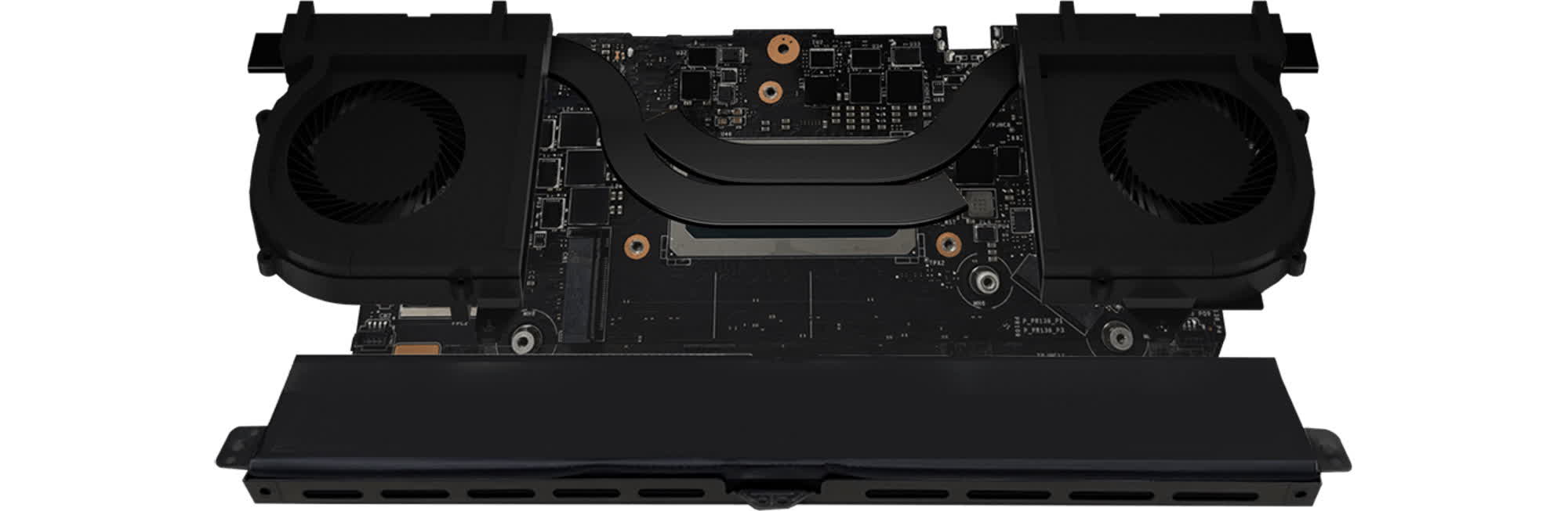
Facepalm: MSI is expected to launch its latest gaming handheld very soon, but people will have to pay a high price if they want one. The Taiwanese corporation tried its best to improve the cost situation, but the supply chain issue in the memory market is not going to disappear anytime soon – and things could become even worse in the not-so-distant future.
MSI should start shipping the Claw 8 EX AI+ on June 23, 2026, slapping a massive $1,800 price tag on the device. The OEM recently explained that the cost is a result of the current state of the memory market, and that more price hikes could arrive over the next few months if the supply chain doesn’t improve soon.
The MSI Claw 8 EX AI+ is based on the Intel Arc G3 processor, a powerful APU design that should provide plenty of computing and graphics power in a 65W envelope. Unlike Valve’s Steam Deck, the new handheld focuses on powerful hardware components to offer a “no-compromise” approach to PC-based portable gaming.
According to MSI product marketing manager Andy Chu, the corporation still has “privileged” access to hardware parts compared to a company like Valve. However, this benefit didn’t result in a much different situation in terms of silicon costs or the final price for customers.
All in all, Chu confirmed in a recent interview that 2026 will be a difficult year for both chipmakers such as Intel and OEM manufacturers such as MSI. Device makers are now unable to fully absorb the cost hikes impacting crucial components such as memory chips or storage, which is why consumers are going to pay more for everything no matter the brand.

“All I can say is we have tried every approach to get the memory and also storage at a lower cost,” Chu said in the interview, “like, deepen the relationship between us and also those suppliers, like to have some deals.” In the end, MSI executives “have done everything we can do to make our system as affordable as possible.”
Despite the high-profile effort, the Claw 8 EX AI+ will still carry its $1,800 price tag. MSI is now trying to change the narrative, highlighting how the new handheld is a high-end gaming device targeting enthusiasts who can spend that kind of money to get a luxury x86 machine. Even the “affordable” Steam Deck is now carrying a significant price premium, which is why MSI hopes customers will take a closer look at a device’s potential in terms of performance and capabilities before placing their order.
Chu is also warning that market conditions could even worsen compared to where they are today. According to his assessment, there is room for yet another price increase related to the supply chain crisis caused by the AI industry. Still, MSI expects sales of its handheld products to remain relatively stable even when factoring in a pricey offering such as the Claw 8 EX AI+.
Microsoft found a USB worm active since February that hijacks clipboards to swap crypto wallet addresses and routes stolen data through a portable Tor client.
Microsoft Threat Intelligence has identified a new strain of self-propagating malware that spreads through USB drives, monitors the Windows clipboard for cryptocurrency wallet addresses and seed phrases, and routes all stolen data through a portable Tor client to avoid detection. The campaign has been active since at least February 2026, according to Microsoft’s analysis published this week.
The malware, which Microsoft detects as Trojan:Win32/CryptoBandits.A, works as a classic USB worm with a modern payload. When a user plugs in an infected drive, they see what appear to be their usual document files. The originals have been hidden, replaced by Windows shortcut (.lnk) files bearing the same names that silently execute the malware when opened.
The .lnk files scan the drive for documents with .doc, .xlsx, and .pdf extensions, hide the originals, and create matching shortcut files in their place. The worm component also writes itself to any new USB drive connected to an infected machine, allowing it to spread further without user action beyond opening what looks like a normal file.
The 💜 of EU tech
The latest rumblings from the EU tech scene, a story from our wise ol’ founder Boris, and some questionable AI art. It’s free, every week, in your inbox. Sign up now!
Once running on a system, the malware deploys a portable Tor client renamed ugate.exe and configures a SOCKS5 proxy on localhost port 9050. All command-and-control traffic then routes through Tor’s .onion network, making it significantly harder for corporate firewalls and security tools to intercept or trace the communications. The C2 infrastructure uses three endpoint paths: /route.php for check-ins, /recvf.php for uploading stolen files, and /stub.php for downloading additional payloads.
The clipboard monitoring is the malware’s primary theft mechanism. It checks the Windows clipboard approximately every 500 milliseconds, looking for patterns that match cryptocurrency wallet addresses or recovery phrases. When it detects a match, it silently replaces the copied address with one controlled by the attacker, so the victim unknowingly sends funds to the wrong wallet.
The malware targets six cryptocurrencies across multiple address formats. For Bitcoin, it recognises legacy addresses starting with “1,” Pay-to-Script-Hash addresses starting with “3,” native SegWit addresses starting with “bc1q,” and Taproot addresses starting with “bc1p.” It also targets Tron addresses beginning with “T” and Monero addresses beginning with “4” or “8.” Clipboard hijacking for cryptocurrency theft is not limited to Windows, with Android trojans like Rokarolla using the same technique to redirect crypto payments on mobile devices.
Beyond wallet addresses, the malware scans clipboard content for BIP39 seed phrases, the 12- or 24-word recovery keys that grant full access to a cryptocurrency wallet. It also extracts Ethereum private keys and Bitcoin Wallet Import Format (WIF) keys. Capturing a seed phrase or private key gives attackers complete control over the associated wallet, not just the ability to redirect a single transaction.
The malware includes a surveillance module that captures five screenshots over a ten-second interval, packaging them for upload to the C2 server. This gives the operators a visual record of what the victim was doing at the time of infection, potentially revealing additional credentials, open browser tabs, or financial dashboards.
A command called EVAL allows the C2 operators to push and execute arbitrary code on infected machines, turning the cryptocurrency stealer into a general-purpose remote access tool. Microsoft notes this capability means the threat actors can adapt the malware’s behaviour after deployment without needing to reinfect the target.
The malware employs multiple layers of evasion. The initial installer is a Python-based executable obfuscated with PyArmor and packaged with PyInstaller, making static analysis difficult. The JavaScript payloads dropped to C:\Users\Public\Documents use a separate dual-layer obfuscation scheme.
As an anti-analysis measure, the malware checks whether Task Manager is running and exits if it detects the process, a basic but effective way to frustrate casual investigation.
The use of Tor for C2 communications reflects a broader shift in malware infrastructure toward anonymisation networks that resist takedown efforts. Traditional malware that relies on fixed domains or IP addresses can be disrupted when defenders seize those assets. Tor-based C2 channels are substantially harder to shut down because the .onion addresses are not tied to any registrar or hosting provider that can be compelled to act.
Microsoft recommends several mitigations, starting with disabling AutoRun and AutoPlay to prevent automatic execution when USB drives are connected. Group Policy can be configured to block .lnk files from running on removable media, and restricting wscript.exe and cscript.exe through application control policies prevents the JavaScript-based payloads from executing.
Network monitoring for connections to localhost port 9050 can flag machines where the portable Tor client has been installed.
USB-borne malware had largely fallen out of the security spotlight as cloud storage and collaboration tools reduced reliance on physical drives. But supply chain and trust-exploitation attacks remain effective precisely because they target behaviours users consider routine, whether that is plugging in a USB drive or installing a package from a familiar repository.
Microsoft published SHA-256 indicators of compromise, MITRE ATT&CK technique mappings, and KQL hunting queries in its blog post to help security teams detect existing infections. The company says Microsoft Defender detects the malware family, and its Defender Experts team assisted in the investigation. Microsoft did not attribute the campaign to a specific threat actor or estimate the number of infections.
Deductive AI, a startup that uses AI to catch and resolve bugs in software, has agreed to be sold to enterprise software company Elastic for up to $85 million, according to a person with knowledge of the deal.
Deductive, which was founded in 2023, came out stealth last November when it announced a $7.5 million seed round led by CRV with participation from Databricks Ventures, Thomvest Ventures, and PrimeSet. The investment valued the startup at $33 million, according to PitchBook.
Elastic and Deductive did not respond to multiple requests for comment. TechCrunch will update this article if either company responds.
The sale marks a speedy exit for Deductive, which is operating in a fast-growing sector known as AI site reliability engineering (AI SRE). Building AI-powered SRE tools has become an important area, driven by the massive influx of AI-written code. Replacing manual debugging with AI enables human SREs to shift focus from constantly fixing outages and other problems to spending more time on helping with product development.
The acquisition reflects a broader trend in which established tech incumbents are looking to buy AI-native startups to integrate agentic technologies into their existing product suites, the source told TechCrunch.
Elastic, which went public in 2018, is best known for Elasticsearch, the search and analytics engine that helps organizations store, search, analyze, and monitor large amounts of data in near real time.
The company’s observability software — essentially tools that let engineers monitor software systems and detect security threats — could benefit from Deductive’s tech. According to the source, integrating Deductive’s AI technology into Elastic will enhance its observability platform by giving customers tools to automatically monitor performance and resolve system failures in real time.
Deductive was co-founded by Rakesh Kothari, who was previously VP of engineering at Lightspeed-backed business analytics startup ThoughtSpot, and Sameer Agarwal, who formerly worked at Apache Software Foundation and Meta. Agrawal was one of the founding engineers at Databricks.
While Deductive reached roughly $1 million in annual recurring revenue (ARR,) according to the source, the startup’s growth lagged behind Resolve AI, one of the sectors’ perceived early winners. The two-year-old Resolve was co-founded by former Splunk executive Spiros Xanthos and Mayank Agarwal. The Greylock and Lightspeed-backed startup was last valued at $1.5 billion when it raised a $40 million Series A extension in April.
When you purchase through links in our articles, we may earn a small commission. This doesn’t affect our editorial independence.

Apple TV will stream an entire Formula 1 race weekend free to U.S. viewers for the first time, opening every Austrian Grand Prix session to fans without a subscription.
Viewers in the United States will be able to watch all Formula 1 Austrian Grand Prix sessions live through Apple TV at no cost. The free access runs from June 26 through June 28 and includes every on-track session, from practice and qualifying to Sunday’s Grand Prix.
The schedule begins with Practice 1 at 7:30 a.m. Eastern on June 26, followed by Practice 2 at 11 a.m. Practice 3 starts at 6:30 a.m. on June 27, with qualifying at 10 a.m. The Austrian Grand Prix is scheduled to begin at 9 a.m. Eastern on June 28.
Apple said the Austrian Grand Prix marks the first time it has made an entire Formula 1 race weekend available free to viewers in the United States. The company has offered free sports programming before, but this promotion includes every Formula 1 session across a race weekend rather than a single event.
Opening every Formula 1 session to non-subscribers gives fans a chance to follow the entire race weekend, not just Sunday’s Grand Prix. Practice sessions shape car setups and race strategy, while qualifying determines the starting grid.
The promotion arrives as Formula 1 continues to draw a larger audience in the United States. Following a full race weekend typically requires access to paid television or streaming services.
The Austrian Grand Prix gives casual viewers a chance to watch every session without paying for access.
The free weekend also gives Apple a chance to put Apple TV in front of viewers who may not regularly use the platform. Fans can follow the weekend from practice through qualifying and the Grand Prix itself.
Apple hasn’t said whether similar free Formula 1 weekends will follow. For now, the Austrian Grand Prix is Apple’s first effort to make an entire Formula 1 race weekend available free to U.S. viewers.

An anonymous reader shared this report from the Associated Press:
Officials in Kansas City, Missouri, are preparing to equip cameras on some public buses with facial recognition software capable of identifying passengers who appear on a list of banned riders or missing persons. Supporters and opponents alike view the effort as a major litmus test for tapping the AI-powered software on a U.S. public transportation system, positioning Kansas City as the latest epicenter of a fierce debate over whether the safety benefits of artificial intelligence are worth the privacy costs.
“The idea of running face recognition on a camera that is pointed on live spaces in public is a line that until recently has never really been crossed in the last 25 years,” said Jay Stanley, senior policy analyst for the Project on Speech, Privacy and Technology at the American Civil Liberties Union. The state of Missouri declined to help fund the project as expected due to concerns with the facial recognition component. Still, the city is pushing ahead with local and federal money, said Tyler Means, chief mobility and strategy officer at the Kansas City Transportation Authority. “Privacy is always a tricky thing,” Means said. “We’ve always had cameras on our buses. It’s just new technology. I think in time it’ll smooth over and people will realize, ‘Well, it didn’t really feel any different’….”
Images captured by cameras aboard the buses would immediately be checked against any active alerts, generated when a missing person, banned rider or someone on a law enforcement watch list designated by the transportation authority is identified… After the buses return to the depot, the transportation authority would archive the regular video footage on a local server for up to five years.
The company partnering with Kansas City to run the cameras “started using live facial recognition years ago to alert nursing homes when residents left the building,” according to the article, and then “brought the technology to correctional institutions and schools.” But this is its first attempt at bringing its cameras onto public transportation.
The article also includes this quote from Will Owen, communications director for the Surveillance Technology Oversight Project. “City residents should not be guinea pigs for transit systems to test Silicon Valley’s latest unproven, biased surveillance tech.”
On June 11, Kalshi released a buzzy ad featuring noted New York Knicks fan Timothée Chalamet. It was a zeitgeist-capturing moment for prediction markets, akin to the 2022 Super Bowl, when seemingly every commercial featured a celebrity shilling crypto.
Yet when I brought Chalamet’s spot up with attendees at Manifest, a recent festival for prediction markets, I was mostly met with blank stares. These conference goers—a mix of academics, startup founders, job seekers, and players in the markets—hadn’t even heard about it. They were too busy thinking about the bigger picture and the risks facing markets.
Their confusion was the perfect encapsulation of a battle that I observed again and again that weekend: The way forecasting philosophers see the markets (tools for the greater good) is very different from how the vast majority of the world sees them (a way to bet on sports).
“We were all waiting for so long to be in the world we’re in now,” Dan Schwarz, the cofounder and chief executive officer of FutureSearch, an artificial intelligence research and prediction startup, tells me. But the platforms have run into problems, from insider trading to sports contracts that, Schwarz worries, are fueling addiction. To outweigh these harms, “prediction markets would have to deliver a lot more value than they are now.”
The prognosticators, it turns out, are concerned that the very thing that’s made prediction markets a global phenomenon could be their undoing.
This year’s iteration of Manifest took place at Lighthaven, an idyllic compound in Berkeley, California. The campus, which takes up about half a city block, also functions as the epicenter of the rationalist movement, which, among other things, prioritizes the safe development of AI and effective altruism.
The vibe skewed heavily male but was still eclectic. Clusters of twenty- and thirty-somethings huddled over laptops in the Tudor-style main house, and someone told me I looked like a guy who would have a stick of gum. Talks about markets jostled for attention alongside sessions about the odds that AI will kill us all and lessons on how to optimize your sex life. There was a furry meetup and watch parties for the first US World Cup match and game 5 of the NBA Finals. (I couldn’t find anyone who had put money on either event, though a few attendees told me they knew of folks who had made bank.) There were markets on play-money platform Manifold about the festival itself, like whether someone would break a bone (still unresolved) and whether Caroline Ellison would show up (yes).
Still, the broader background conditions were wildly different from previous years. Though Kalshi and Polymarket had sponsored the event in past years, they were AWOL this year. Both companies declined to comment on the change. Last year, Kalshi held a session on sports markets, which it had launched just six months earlier. This year, the companies are facilitating billions of dollars in sports trades during an especially friendly political era at the national level.
Sports were also conspicuously absent during a session on strategies for mastering markets around world events and politics. I caught up with David Bensoussan, the session’s organizer, who has made $1.6 million in profits on the platform, under the boughs of one of Lighthaven’s trees.
“The truth-seeking mechanism that prediction markets can have in terms of predicting things and making the population more informed—what on Earth does that have to do with sports?” he asks, wrapped in a blanket to ward off the chill of Bay Area shade.



No Jackpot Winner as $257 Million Prize Rolls Over to $269 Million Monday Draw

Weekend Open Thread: Miami – Corporette.com

Zimbabwe Requires Crypto Businesses to Register Annually Under New FIU Regulations

Wall Street Week Ahead: Investors see Micron earnings as pulse check of AI rally momentum

Matt Damon’s Viral Sci-Fi Thriller Has Taken Over HBO Max


As AI companies race to go public, who else is along for the ride?


Anthropic staff to meet White House officials next week, Axios reports

HIVE shares jump as $220M AI deal speeds Bitcoin mining pivot

Bitcoin could crash to $48,000, if this historical pattern is triggered
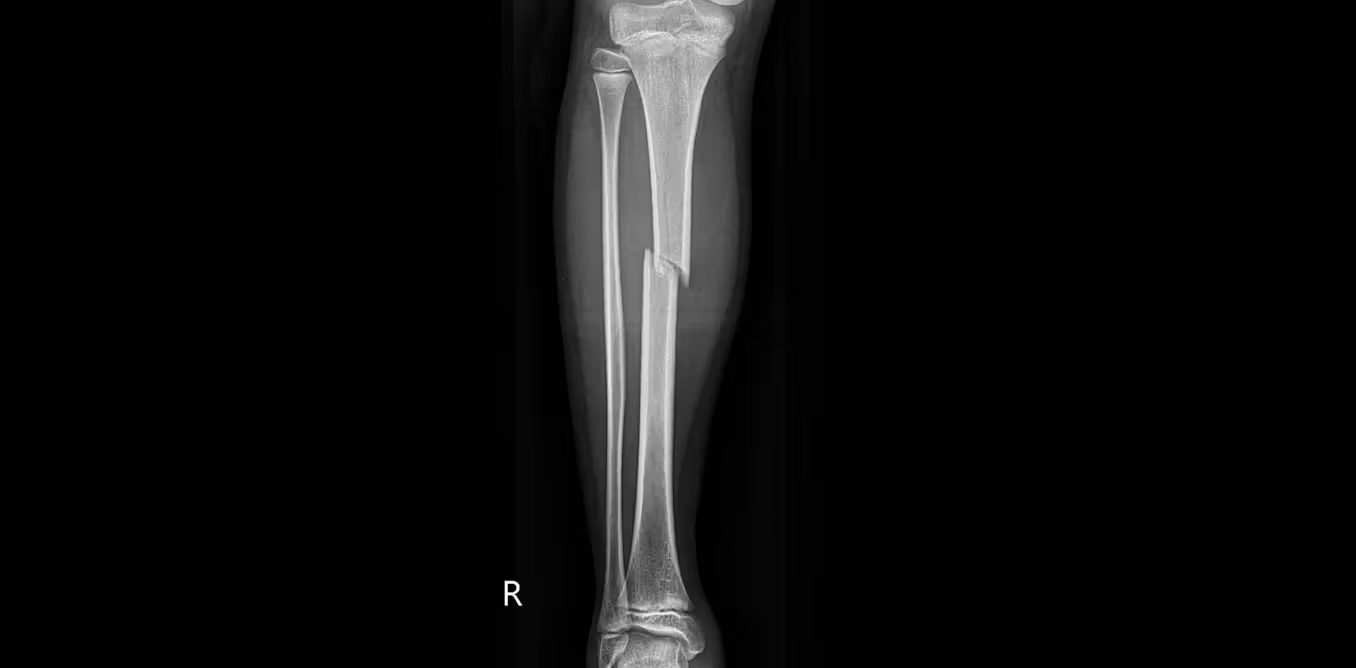
what doctors are seeing in ebike crashes

Warning of disruption as Cardiff Crossrail works to start

Tributes to former deputy head teacher at Cambridge school among death and funeral notices

Kate Middleton Glare Goes Viral After Kids Booed At Royal Event


“Israel’s” ban on ICRC visits ruled illegal, but Knesset moves to stop them permanently


Financial Accounting | Last Day Revision Strategy and Booster | CMA Inter – June 2026


XRP ETFs Outperform As Bitcoin And Ethereum Funds Extend Outflow Trend


Over 400 Arch Linux packages compromised to push rootkit, infostealer


Invesco Quality Income Fund Q1 2026 Commentary


Singer Oliver Tree dies aged 32 in helicopter crash in Brazil

Market Preview: SpaceX (SPCX) IPO Record, Federal Reserve Meeting, and Iran Nuclear Agreement
You must be logged in to post a comment Login